


To meet the electronics industry’s growing demands for scale, cost control, and reliability, PCB manufacturing has evolved into multiple process routes. Each method differs in material compatibility, upfront investment, volume economics, and the wiring density it can support.
This guide summarizes six widely used PCB manufacturing methods so readers can quickly understand the basic workflow, key advantages and tradeoffs, and where each approach is typically used.
1. Stamping / Punching: A Low-Cost Path for High-Volume Single-Sided PCBs
Stamping (punching) forming is most commonly used for low-cost, single-sided PCBs, often found in certain consumer electronics.
How it works (high-level)
- The circuit pattern is created first .
- A cost-effective substrate is commonly used, such as paper-fiber-reinforced epoxy.
- Holes are formed by a punch die .
- The board outline is created using a second die that “punches out” the PCB shape from a larger panel.
Panelization and “depaneling” cost savings
In high-volume production, manufacturers often build multiple boards within a single production panel to reduce handling and processing costs.
- A standard production panel typically contains multiple identical PCBs.
- After assembly and testing, boards are separated from the panel in a controlled process commonly referred to as depaneling .
- This approach reduces labor, handling, and throughput cost—helping keep unit pricing low.
Best fit applications
- Single-sided, cost-sensitive, high-volume products
- Not ideal for high-density interconnect designs, complex materials, or multi-layer builds
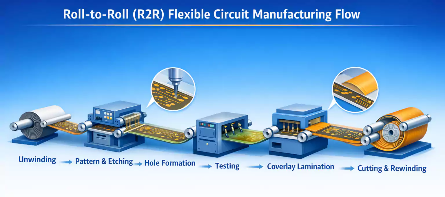
2. Roll-to-Roll (R2R): The Lowest-Cost Route for Mass-Produced Flexible Circuits
Roll-to-roll (R2R) manufacturing is a classic method for producing large quantities of flexible circuits (FPCs). It is often considered one of the lowest-cost approaches for flex—when volume is high enough.
Key characteristics
- Low unit cost in scale, but requires significant tooling and process setup, making it best suited to very high-volume programs.
- Flexible circuits produced via R2R may be single-sided or double-sided.
Typical applications
Examples often associated with R2R-style flex production include:
- Printhead interconnect circuits
- Disk drive head interconnects.
- Internal circuits in cameras and camcorders
Process flow (similar to continuous printing)
R2R production resembles newspaper printing: a long roll of copper-clad laminate moves through a continuous line, typically including:
- Conductor pattern printing
- Etching
- Hole formation
- Testing
- Cutting/separating circuits from the roll (slitting into sheets/strips)
In addition, the process often includes laminating a coverlay over insulation and conductor surfaces for:
- Electrical insulation
- Surface protection
- Improved mechanical durability
3. Lamination: The Foundation of Multilayer PCBs (More Than Two Layers)
Once a PCB requires more than two layers, lamination becomes essential. Lamination bonds multiple patterned layers into a single consolidated board.
Standard workflow (high-level)
A) Build inner layers (“cores”)
- Inner-layer conductor patterns are etched on laminate sheets.
- These etched inner-layer laminates are commonly referred to as cores.
B) Stack-up using prepreg and copper foil
- Cores are separated by prepreg layers (resin-impregnated fiberglass).
- The stack is arranged according to the required layup / stack-up design.
- Copper foil is placed on the outside to form the outer layers.
C) Heat and pressure to flow and cure resin
- The stack is pressed in a lamination press.
- Heat softens and flows the prepreg resin, filling gaps around copper features and bonding the layers.
- After cooling, the resin cures, forming a rigid multilayer production panel.
D) Downstream steps
- After lamination, the panel typically proceeds to drilling and plating (for plated-through holes and related interconnect features).
Special material note (polyimide and similar)
Some materials, such as polyimide (PI), may not use the same prepreg bonding approach in all builds. In those cases, manufacturers may use special adhesives during lamination to achieve reliable layer bonding.
4. Subtractive Process: The Dominant Way to Form Copper Patterns
The subtractive process is the classic and most widely used method for forming copper traces in PCB manufacturing.
Core concept
- Start with a laminate that has a full sheet of copper.
- Apply a resist layer to protect the copper that should remain.
- Run the panel through an etching process to remove unprotected copper.
- Result: unwanted copper is “subtracted,” leaving behind the required conductor pattern.
Why is it so common
- Mature, well-understood process
- Broad equipment ecosystem and strong supply chain support
- Suitable for a wide range of traditional PCB designs and production needs
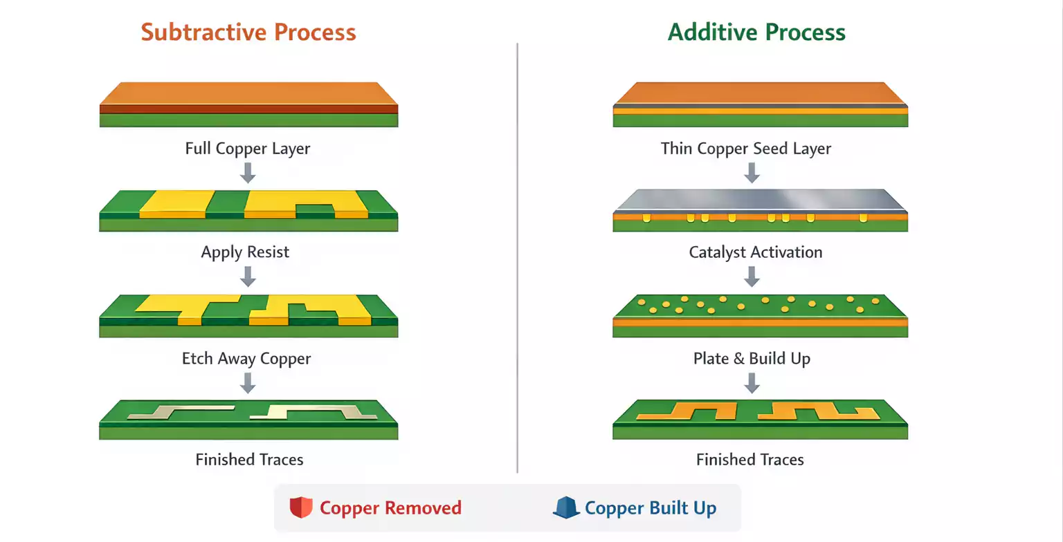
5. Additive Process: “Building Up” Copper Where You Need It
The additive process works in the opposite direction from subtractive etching. Instead of starting with thick copper everywhere, additive processing aims to deposit copper only where needed, then build it up to the target thickness.
High-level approach
A typical additive route includes:
- Preparing target areas for deposition (often by chemical activation/sensitization steps)
- Depositing a thin electroless copper layer to create an initial conductive path
- Using electroplating to thicken copper in the desired areas to reach the final conductor thickness
Why it matters
Additive methods are often viewed as a way to reduce material waste and lower some chemical consumption compared with removing large amounts of copper through etching, though practicality depends on the specific product and process capability.
6. Discrete Wiring (Multiwire): A Niche Way to Create Routing Layers
Discrete wiring, often called multiwire, is a less common method of forming routing layers.
Basic idea
- Round metal wires are embedded or rolled into a soft insulating material to form the routing layer.
- This insulating layer is applied over a power-plane core, effectively building a wiring structure around the power-layer foundation.
Industry adoption
Only a small number of manufacturers use multiwire techniques today. Compared with mainstream multilayer processing, its advantages are generally limited to niche applications and specific design constraints.
How to Think About These Methods at a Glance
- Stamping / Punching: Best for low-cost, single-sided boards at high volume—fast mechanical hole and outline forming.
- Roll-to-Roll: A go-to for mass-produced flexible circuits, with excellent cost efficiency at very high volume.
- Lamination: The backbone of multilayer PCB fabrication—combines cores, prepreg, and outer copper foils under heat and pressure.
- Subtractive: The most common copper pattern method—protect what you want, etch away the rest.
- Additive: Deposit and build copper where needed—can reduce waste depending on implementation.
- Discrete Wiring (Multiwire): A specialized, less common wiring-layer approach using embedded metal wires.
Conclusion
Choosing the right PCB manufacturing method comes down to three factors: board type, production volume, and density requirements. Align these early with your fabricator’s capabilities to reduce risk, control cost, and improve yield. For deeper detail, explore our related guides on PCB stack-ups, via structures, and flex vs. rigid-flex design.