Gold-finger PCB is designed for reliable edge-connector contact and repeated insertion cycles. They’re widely used in edge-card modules, plug-in interface boards, backplanes, test adapters, and industrial/computing expansion cards—where stable mating and low contact resistance matter.
FastTurn PCB delivers precision gold-finger PCB fabrication with controlled nickel and hard gold plating, optional bevel/chamfer edge processing, and engineering-led DFM checks to prevent wear, oxidation, and fit issues.
Why Gold Fingers
High conductivity for stable contact
Strong oxidation resistance
Wear-resistant surface for frequent mating
Prototype to Production
Fast-turn prototypes and high-mix builds
Small-to-medium production runs
Bare PCB delivery with optional impedance control and assembly-ready panelization/edge processing support
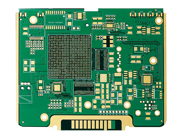
What Is a Gold Finger PCB (Edge Fingers) ?
A gold finger PCB features gold-plated contact pads along its edge. These edge contacts slide into a mating connector to create a low-resistance, reliable electrical interface—essential for boards that are plugged in and removed repeatedly.
Gold Fingers vs. Edge Connector
Gold fingers: the plated pads on the PCB edge
Edge connector: the mating connector hardware that the PCB plugs into
Why “Hard Gold” Is Common
For edge contacts, hard gold (electroplated gold over nickel) is often specified because it offers:
Higher wear resistance for repeated mating cycles
Strong oxidation resistance for long-term contact stability
Consistent conductivity at the connector interface
Gold Finger PCB Capabilities
FastTurn PCB supports gold finger (edge connector) builds with controlled plating, precise edge processing, and DFM-driven manufacturability checks to help ensure reliable mating and long service life.
Plating & Surface Finish Options
Electroplated Nickel + Hard Gold Built for connector frictionand frequent insertion/removal, where wear resistance matters most.
ENIG (Electroless Nickel Immersion Gold) A practical alternative when high wear resistance isn’t required,and the edge contact is used less frequently.
Gold Finger Types
Regular / Flush Fingers– Standard edge contacts for typical card-edge interfaces
Segmented / Intermittent Fingers– Spaced contact groups used for specific connector layouts
Long-Short / Uneven Fingers– Staggered lengths to support controlled sequencing during insertion
Bevel / Chamfer Edge Processing
Beveling helps guide the PCB into the connector, reduces insertion wear, and improves mating consistency.
Purpose:smoother insertion and improved connector engagement
Angle options: Available as selectable specifications based on connector requirements
Solder Mask Opening & Keep-Out Rules
To protect contact performance and plating quality:
No solder mask or silkscreenon the gold finger plating area
Continuous solder mask openingis recommended for clean plating boundaries.
Maintain a keep-out zonenear the fingers to avoid features too close to the edge and reduce risk during edge processing.
Design Guidelines for Gold Fingers
Keep-Out Near the Board Edge
Keep copper, vias, and other features away from the gold finger edgeto protect routing and bevel processing.
Reserve a local keep-out zonearound the finger area for stable plating and clean edges.
Copper Near the Bevel/Chamfer
Avoid traces/pours in the bevel path.
If needed, specify copper removalnear the edge to prevent exposure or defects after chamfering.
Solder Mask & Silkscreen
No solder mask or silkscreenon the gold finger plating area.
Use a continuous mask openingfor clean plating boundaries.
Hard Gold vs. ENIG
Hard Gold:frequent insertion/removal, higher wear resistance.
ENIG:limited mating cycles, wear resistance not critical.
Testing & Inspection for Reliable Contacts
Gold finger PCBs depend on clean plating, precise edge geometry, and stable electrical continuity at the connector interface. FastTurn applies inspection and testing steps throughout fabrication to help ensure your edge contacts perform reliably in real-world mating conditions.
Inspection Focus
Visual Inspection of Plating & Edge Definition Checks for uniform coverage, clean boundaries, and consistent finger geometry.
Bevel/Chamfer Verification (When Specified) Confirms edge finishing meets the drawing callout for smooth connector insertion.
Solder Mask Opening & Keep-Out Review Verifies the gold finger region is free of mask/silkscreen and maintains required clearances.
Electrical Testing
100% Electrical Test (E-Test) Validates opens/shorts and net connectivity before shipment—critical for edge-connector boards.
Optional Impedance Verification For high-speed edge interfaces, impedance targets can be supported based on stackup and trace rules.
Quality & Certifications
FastTurn PCB enforces strict quality and process control standards to ensure consistent plating, edge accuracy, and contact reliability across all gold finger PCB projects. From incoming materials to final inspection, our manufacturing follows IPC-based guidelines and documented procedures to deliver edge-connector PCBs that meet your performance and durability expectations.
Quality at Every Step
We apply structured controls across every stage of gold finger PCB fabrication:
Standardized Plating & Beveling Processes
Defined parameters for hard gold thickness, bevel angle, and copper clearance.
Visual & Electrical Inspection
AOI and E‑test to ensure plating quality, outline integrity, and signal continuity.
IPC-Based Workmanship Standards
Manufactured in alignment with IPC guidelines for surface finish, edge geometry, and plating reliability.
Process Documentation & Traceability
Internal record keeping for plating specs, inspection results, and batch-level control.
Continuous Improvement Practices
Ongoing process optimization through internal audits, training, and lean manufacturing methods.
Certifications
FastTurn PCB maintains quality systems and industry compliance to support high-reliability builds:
Our portfolio includes gold-finger PCBs (edge connector boards) with hard-gold fingers and optional beveled/chamfered edges, designed for reliable mating and long service life. Typical projects include edge-card modules, interface boards, and backplanes—delivered from prototypes to small- to medium-sized production runs.
Prototyping to Production
FastTurn PCB supports the full lifecycle of gold finger PCB manufacturing—from fast-turn prototypes to scalable production—so you can validate connector fit and contact performance early, then ramp with consistent process control.
Gold finger builds often require tighter coordination on plating type (hard gold vs ENIG), solder mask openings, and optional bevel/chamfer callouts. Our DFM review helps confirm these details up front, reducing respins and protecting mating reliability during scale-up.
Our Agile Manufacturing Model Supports
NPI (New Product Introduction) Structured support for early builds and production ramp.
Rapid Design Validation Fast feedback on manufacturability for fingers, edge processing, and panel strategy.
High-Mix, Low-Volume Builds Prototype-friendly workflows for diverse connector designs.
Small-to-Medium Production Runs Repeatable plating and edge processing for stable output.
Accelerated Time-to-Market Streamlined quoting and controlled fabrication to keep schedules on track.
Industries & Applications We Support
We serve a diverse range of industries with precision-built gold finger PCBs, engineered to deliver reliable edge-connector contact, strong wear and oxidation resistance, and consistent performance across repeated insertion cycles.
FastTurn PCB offers gold-finger PCB manufacturing for applications that require reliable edge-connector contact, wear resistance, and stable electrical performance across repeated insertion cycles. Through controlled nickel and hard gold plating, optional bevel/chamfer edge processing, and consistent inspection, we deliver edge connector PCBs that meet application-specific requirements.
Industries & Applications
Aerospace & Defense
Medical & Life Sciences
Industrial & Automation
Communications & Networking
Computing & Data Systems
Energy & Power Systems
Why FastTurn PCB?
FastTurn PCB delivers high-reliability gold finger PCBs built on precision plating, controlled edge processing, and engineering-driven execution—supporting the full lifecycle from prototype to production.
Diverse Industry Expertise
We support industrial, medical, energy, communications, and other high-reliability industries, delivering through-hole PCB assembly and mixed-technology PCBA for applications with demanding mechanical and environmental requirements.
End-to-End PCB Assembly Solutions
FastTurn provides end-to-end PCB assembly services under one controlled workflow. Early DFM involvement helps reduce risk and enables a smooth transition from fast-turn prototypes to scalable production.
Turnkey Assembly Services
Our turnkey PCB assembly services include component sourcing, SMT and through-hole assembly, testing, and final integration—simplifying supply chains and improving execution consistency.
Advanced Manufacturing Capabilities
We support complex PCB assemblies through controlled processes, skilled technicians, and flexible assembly lines suited for high-mix and low-to-medium volume production.
Comprehensive Testing & Quality Control
Quality is embedded throughout our PCB assembly process, with inspection and testing methods applied to detect issues early and ensure long-term reliability.
Efficient Lead Times
Streamlined workflows and responsive engineering enable fast prototype turnaround and reliable production schedules without compromising assembly quality.
Inside Our Facilities
Our manufacturing floors support gold-finger PCB fabrication with dedicated process control for nickel-hard gold plating, precision edge profiling, and optional bevel/chamfer finishing. Backed by IPC-based process discipline and RoHS-compliant options, we maintain consistent plating quality, clean edge definition, and reliable execution across every build.
FAQ
What is a gold finger in a PCB?
Gold fingers are gold-plated contact pads on the PCB edge that mate with an edge connector.
Gold fingers vs. edge connector—what’s the difference?ring?
Gold fingers are the pads on the PCB. The edge connector is the mating connector part.
Hard gold vs ENIG—what should I choose?
Hard gold (electroplated):best for frequent insertion/removal and wear resistance.
ENIG:suitable for limited mating cycles.
Do I need a bevel/chamfer for gold fingers?
Often yes. Beveling helps smooth insertion and reduces wear on the contacts and connector.
What electronics use gold fingers?
Common in expansion cards, backplanes, plug-in modules, and memory-style edge cards.
Looking for an expert quick-turn to turnkey PCB solution?
FastTurn PCB specializes in higher layer count PCBs, quick-turn manufacturing, HDI structures, blind and buried vias, as well as controlled impedance and precision fabrication processes.