Multilayer PCB Manufacturer & Fabrication
High-quality multilayer PCB boards engineered for dense routing and stable signal integrity. As a reliable multilayer PCB supplier, we combine stackup-focused DFM feedback with controlled lamination and drilling processes to support fast-turn prototypes and scalable production.
- All uploads are secure and confidential.


Precision Multilayer PCB Manufacturing Services?
What Is a Multilayer PCB?
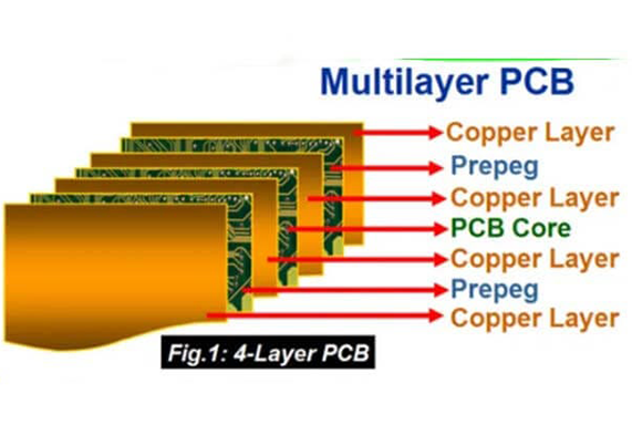
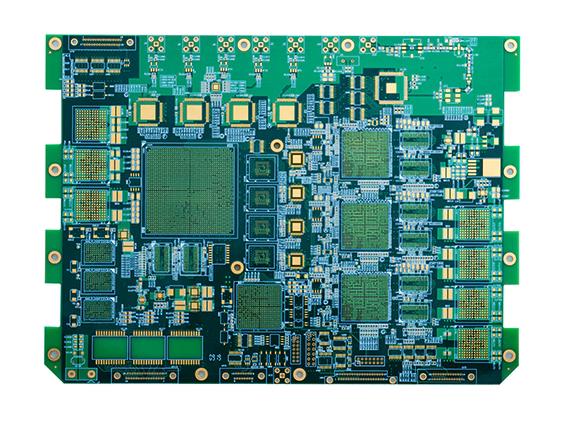
A multilayer PCB (multilayer printed circuit board) is a circuit board with more than 2 copper layers—most commonly 4 or more. These layers are laminated together with insulating dielectric materials, creating a compact structure that supports higher routing density and more complex circuit functions than single- or double-sided boards.
Multilayer PCB manufacturing typically includes inner-layer imaging and etching, lamination (pressing) to form the stackup, and drilling and copper plating to create electrical connections between layers via vias. By combining signal layers with dedicated power and ground planes, multilayer PCB boards can improve return paths, reduce noise, and support stable electrical performance in demanding designs.
Multilayer PCBs are widely used in industrial control, communications and networking, medical electronics, automotive systems, and other applications where compact layout, consistent performance, and reliability are critical. When signal integrity, EMI control, or circuit complexity exceeds the limits of 2-layer designs, multilayer PCB fabrication becomes the preferred solution.
Multilayer PCB Structure & Stackup Basics
A multilayer PCB stackup defines the arrangement of copper and dielectric layers to achieve the required routing density, signal integrity, and mechanical stability. In most designs, the stackup includes signal layers for routing, power/ground planes for low-impedance reference and noise control, and dielectric layers (core/prepreg) that set spacing and impedance behavior.
- Stackup Overview
Signal layers:Route high-speed, mixed-signal, and control traces
Power/Ground planes:Provide stable reference planes, reduce noise, and improve EMI performance
Dielectric layers:Control spacing between layers, affecting impedance and coupling
- Common Stackup Examples
4-layer stackup:Signal / Ground / Power / Signal
6-layer stackup:Adds dedicated planes or extra signal layers for routing and isolation
8-layer stackup:Supports higher density, improved plane segmentation, and better EMI control for complex systems
- Design Notes for Reliable Manufacturing
Return paths:Keep high-speed traces referenced to continuous planes to reduce loop area and noise
Plane strategy:Use solid ground planes where possible; plan splits carefully to avoid return-path disruption
Controlled impedance:Stackup thickness, dielectric properties, and trace geometry should be coordinated for single-ended and differential impedance targets.
Copper balance:Symmetry and copper distribution help reduce warpage and improve lamination stability
Via Types for Multilayer PCBs
Through Vias
Through vias extend from the top layer to the bottom layer, passing through the entire board. They are widely used for general interconnects because they are cost-effective and well-suited for many multilayer PCB designs.
Blind Vias
Blind vias connect an outer layer (top or bottom) to one or more inner layers without going through the full board thickness. They help increase routing density by freeing up space on inner layers and are often used when a compact layout is required.
Buried Vias
Buried vias connect internal layers only and are not visible on the outer surfaces. They can further improve routing efficiency and signal isolation in high-density multilayer PCBs, but require additional lamination steps and tighter process control.
Our Multilayer PCB Capabilities

FastTurn PCBs provides comprehensive multilayer PCB manufacturing and multilayer PCB fabrication capabilities to support high-density designs that require consistent stackup control, reliable interconnects, and stable electrical performance. Our workflows are built to handle a wide range of board constructions and production needs—from quick-turn prototypes to scalable production.
- Layer Count & Build Complexity
We support multilayer PCB builds from early prototypes through production scaling, accommodating common multilayer stackups such as 4-layer, 6-layer, and 8-layer boards, as well as higher-complexity designs when required.
- Board Thickness & Copper Weight Options
Multiple board thickness and copper weight options are available to match mechanical requirements, current carrying needs, and thermal constraints—helping optimize reliability without overbuilding.
- Fine-Line Routing & Hole/Via Features
Our multilayer PCB fabrication supports dense routing and robust interlayer connectivity, with controlled processes for drilling, plating, and layer-to-layer registration. Capability selection is guided by DFM review to balance performance, yield, and cost.
- Materials Selection
We manufacture multilayer PCB boards using standard FR-4 and can support high-TG or low-loss materials based on thermal requirements or signal integrity requirements.
- Surface Finishes
We offer standard surface finishes used in multilayer PCB manufacturing, such as HASL, ENIG, OSP, and other options as needed—selected based on solderability, reliability, and end-use conditions.
Multilayer PCB Manufacturing Process
Our multilayer PCB manufacturing process is built around stackup accuracy, repeatable interlayer connectivity, and consistent quality control. Below is a typical workflow used for multilayer PCB fabrication—from engineering review to final verification.
- Inner Layer Imaging & Etching
Inner-layer circuits are transferred and etched to form the required trace patterns. Tight control at this step helps ensure routing accuracy for dense multilayer PCB boards.
- Lamination (Pressing)
Inner layers are aligned with prepreg/core materials and laminated under controlled pressure and temperature to form the multilayer stackup. Proper registration and stack symmetry support stable build quality.
- Drilling & Plating
Holes and vias are drilled and then copper-plated to create reliable electrical connections between layers. Process control here is critical for via integrity and long-term reliability.
- Outer Layer Patterning
Outer-layer traces and pads are formed through imaging and etching, completing the primary circuit structure on the top and bottom layers.
- Solder Mask & Surface Finish
Solder mask is applied for insulation and protection, followed by the selected surface finish (such as HASL, ENIG, or OSP) to ensure solderability and meet end-use requirements.
- Electrical Test & Final Inspection
Each multilayer PCB build undergoes electrical testing to verify continuity and isolation, followed by a final inspection to confirm artistry and conformance before shipment.


Advanced Testing for Maximum Reliability
Reliable multilayer PCB performance requires verification—not just precise fabrication. FastTurn integrates inspection and electrical testing into multilayer PCB manufacturing to catch defects early and ensure boards meet build and electrical requirements.
Testing is applied for both prototypes and low-to-medium production, and is selected based on stackup complexity, layer count, via structures, and performance needs. For controlled-impedance or high-reliability builds, additional verification can be included to improve consistency.
Testing & Inspection Capabilities
- 100% Electrical Testing (E-Test)
Verifies continuity and isolation to identify opens, shorts, and netlist-related issues before shipment. - Automated Optical Inspection (AOI)
Inspects outer-layer features to detect trace defects, spacing issues, and pattern irregularities. - Impedance Verification
Supports designs with controlled impedance targets by validating manufacturing consistency against impedance requirements. - Microsection / Cross-Section Analysis
Evaluates internal build quality—such as plating, layer registration, and via integrity—for higher reliability programs. - Final Visual Inspection
Confirms artistry, surface finish condition, and overall conformance to build requirements.
Quality & Certifications
Quality at Every Step
- Comprehensive Quality Control Systems
- In-Process Inspection & Process Monitoring
- Electrical Testing (E-Test)
- Traceability & Documentation
- Continuous Improvement Practices
FastTurn PCB maintains strict quality, safety, and compliance standards across all multilayer PCB manufacturing projects. Our quality system is supported by in-process inspections, electrical testing, and controlled documentation to ensure consistent reliability and repeatable performance. Quality control is embedded throughout our multilayer PCB fabrication workflow—from incoming materials to final inspection and shipment.
Certifications & Compliance
- ISO 9001:2015 – Quality Management Systems
- ISO 13485:2016 – Medical Device Manufacturing
- IPC-A-610 & J-STD-001 – Assembly Workmanship Standards
- RoHS / Lead-Free Compliance – Environmental Regulations
- ANSI/ESD S20.20 – ESD Protection
- SMTA Membership – Industry Standards Participation
Our portfolio
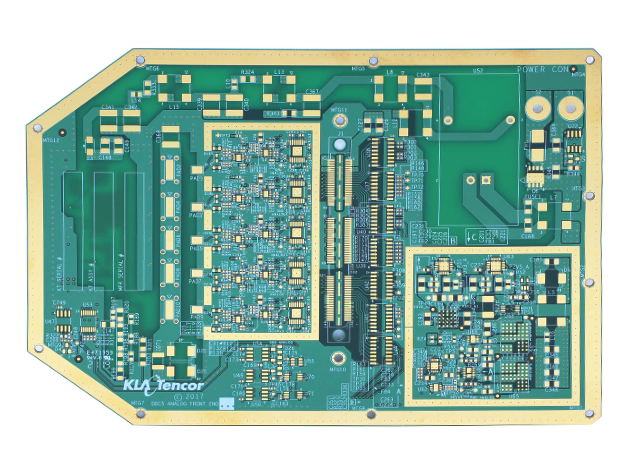
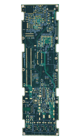
Our portfolio highlights multilayer PCB boards manufactured for performance-driven applications—from standard 4-layer and 6-layer PCBs to more complex multilayer stackups with dense routing and reliability-focused requirements. Each build reflects our focus on stackup consistency and verified electrical performance from prototype to production.


Prototyping to Production
FastTurn PCBs supports the complete multilayer PCB lifecycle—from fast-turn prototypes to scalable production—so you can move from early validation to stable manufacturing with confidence. Our multilayer PCB fabrication process is built to maintain stackup consistency, repeatable via integrity, and verified electrical performance as your volumes grow.
We support engineering prototypes, high-mix builds, and low-to-medium-volume production, adapting scheduling and manufacturing controls to meet project timelines without sacrificing quality.
Our Agile Manufacturing Model Supports
- NPI (New Product Introduction) Programs
Structured support for early-stage designs and production ramp-up. - Design Validation with Rapid Feedback
DFM-focused feedback to improve manufacturability and reduce iterations. - Low- and High-Mix Production Volumes
Flexible multilayer PCB production aligned to varying complexity and demand. - Accelerated Time-to-Market
Streamlined workflows that shorten the transition from prototype to production. - Manufacturability Optimization During Design
Practical guidance on stackup, via structures, and fabrication constraints to improve yield and stability.


Industries & Applications We Support
Industries & Applications We Support
FastTurn PCB provides multilayer PCB manufacturing for applications that demand dense routing, stable electrical performance, and consistent build quality. Our capabilities support complex multilayer stackups used in demanding environments, from fast-turn prototypes to scalable production. Through controlled processes and electrical verification, we deliver multilayer PCBs aligned with application-specific technical requirements.
Industries & Applications
- Industrial & Automation
Multilayer PCBs for control systems and embedded platforms requiring reliability and long service life. - Communications & Networking
Multilayer boards supporting high-speed interfaces and signal integrity–focused designs. - Automotive Electronics
Multilayer PCBs for modules and control units where consistency and durability matter. - Medical Electronics
Multilayer PCBs are built for diagnostic and monitoring devices requiring stable performance and traceability (as required). - Energy & Power Systems
Multilayer PCBs for power management, conversion, and control electronics. - Commercial Electronics
Multilayer boards enable compact layouts and higher functional integration. - Emerging Technologies
Multilayer PCB support from rapid prototyping to production scaling for new product development.
Why FastTurn PCB?
FastTurn PCB delivers high-performance PCB manufacturing solutions built on precision, reliability, and scalability. With integrated capabilities and engineering-driven execution, we support the full product lifecycle from prototype to production.
Diverse Industry Expertise
We support industrial, medical, energy, communications, and other high-reliability industries, delivering through-hole PCB assembly and mixed-technology PCBA for applications with demanding mechanical and environmental requirements.
End-to-End PCB Assembly Solutions
FastTurn provides end-to-end PCB assembly services under one controlled workflow. Early DFM involvement helps reduce risk and enables a smooth transition from fast-turn prototypes to scalable production.
Turnkey Assembly Services
Our turnkey PCB assembly services include component sourcing, SMT and through-hole assembly, testing, and final integration—simplifying supply chains and improving execution consistency.
Advanced Manufacturing Capabilities
We support complex PCB assemblies through controlled processes, skilled technicians, and flexible assembly lines suited for high-mix and low-to-medium volume production.
Comprehensive Testing & Quality Control
Quality is embedded throughout our PCB assembly process, with inspection and testing methods applied to detect issues early and ensure long-term reliability.
Efficient Lead Times
Streamlined workflows and responsive engineering enable fast prototype turnaround and reliable production schedules without compromising assembly quality.
Inside Our Facilities
Our production floors are purpose-built for multilayer PCB manufacturing, featuring controlled inner-layer imaging, precision drilling and plating, and tightly managed lamination and registration processes. Supported by engineering-led DFM, in-process inspection checkpoints, and RoHS-compliant workflows, we ensure consistent quality and repeatable execution across every multilayer PCB build.


FAQ
A multilayer PCB is a printed circuit board with more than 2 copper layers (typically 4 or more) laminated together to support higher routing density and better electrical performance.
They can, but 3-layer PCBs are rare. Most designs use even layer counts (4, 6, 8) for stackup symmetry and manufacturing stability.
The main disadvantages are higher cost and greater fabrication complexity compared to 1–2-layer boards due to lamination, tighter registration control, and additional drilling/plating steps.
A standard “rule” is to use solid reference planes (especially ground) and keep signals referenced to continuous planes for cleaner return paths and improved EMI behavior—often the reason teams move from 2 layers to 4.
- 4-layer:general-purpose, good plane reference
- 6-layer:more routing and isolation
- 8-layer+:higher density and better plane planning for complex systems
The right choice depends on routing density, EMI, and power requirements.
Blind vias connect an outer layer to inner layers, and buried vias connect inner layers only. They increase routing density but add process complexity and cost.
Yes—provide target impedance values (single-ended/differential) and stackup intent, and the build can be reviewed and manufactured to meet impedance requirements.
Looking for an expert quick-turn to turnkey PCB solution?
FastTurn PCB specializes in higher layer count PCBs, quick-turn manufacturing, HDI structures, blind and buried vias, as well as controlled impedance and precision fabrication processes.