


When designing and manufacturing printed circuit boards (PCBs), one of the most important yet often misunderstood layers is the solder mask—also known as solder stop mask or solder resist. Whether you’re a beginner trying to understand what it does or an experienced engineer refining your DFM (Design for Manufacturability) practices, this guide will walk you through everything you need to know: what solder mask is, why it matters, design rules, materials and types, common pitfalls, and how to communicate requirements to your manufacturer for reliable, predictable results.
What Is Solder Mask?
In its simplest definition, a solder mask is a thin protective polymer layer applied to the surface of a PCB that covers copper traces and prevents solder from bridging or forming unintended electrical connections between closely spaced pads during assembly. This layer also protects copper from oxidation, environmental damage, and contamination.
In EDA tools and Gerber CAM files, solder mask layers are defined by negative images: areas where solder mask is not present correspond to exposed pads or vias.
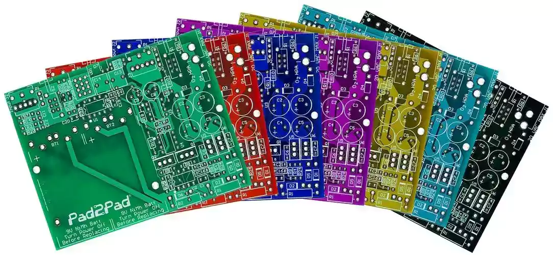
Solder mask is most commonly green, but boards can be manufactured in a range of colors, including red, blue, black, white, yellow, and purple.
Why Solder Mask Matters
A solder mask might seem like cosmetic “green paint” to a novice, but in reality, it plays several critical roles:
1. Prevents Solder Bridging and Shorts
When molten solder flows during assembly, it follows the path of least resistance. Without a solder mask, solder can bridge between adjacent pads or traces, causing short circuits. The solder mask insulates the copper surface and confines solder to designated lands.
2. Protects Against Corrosion and Oxidation
Bare copper exposed to air and moisture oxidizes over time. Oxidation degrades solderability and can increase electrical resistance. A solder mask shields copper from these environmental effects.
3. Reduces Environmental and Mechanical Damage
Solder mask provides a physical barrier that helps prevent scratches, moisture ingress, chemical contamination, and whisker growth that can lead to corrosion or shorts.
4. Improves Assembly Yield
Especially in automated processes such as reflow or wave soldering, the mask layer guides solder to the intended areas, contributing to stable, high-yield production.
Types of Solder Mask and Materials
Not all solder masks are created equal. Different applications and design requirements dictate which type is best suited for your PCB.
Polymer Types
Most solder masks consist of a mixture of:
- Resin (epoxy, polyurethane, acrylic) for the film structure,
- Hardener to crosslink the resin,
- Fillers and dyes for thickness control and color,
- UV-reactive substances for proper photolithography.
Common Mask Formats
Liquid Photoimageable Solder Mask (LPI)
LPI is the most widely used solder mask type in commercial PCB production. It’s coated as a liquid, then exposed with UV light through a photomask and developed to define openings. It is suitable for complex, fine-feature boards and offers good adhesion and resolution.
Dry Film Photoimageable Masks
This format resembles a film laminated onto the board. It offers very uniform thickness and excellent edge definition—beneficial for ultra-fine-pitch or high-density boards—though at a somewhat higher cost.
Epoxy Liquid Masks
Traditional epoxy liquid solder masks are lower-cost but offer lower accuracy and resolution than photoimageable options. For simple boards, they may still be adequate.
Solder Mask Design Guidelines (DFM)
Getting the solder mask right in your PCB design is not just about aesthetics—it directly ties into whether your board can be reliably manufactured and assembled.
Understanding Openings, Clearance, and Expansion
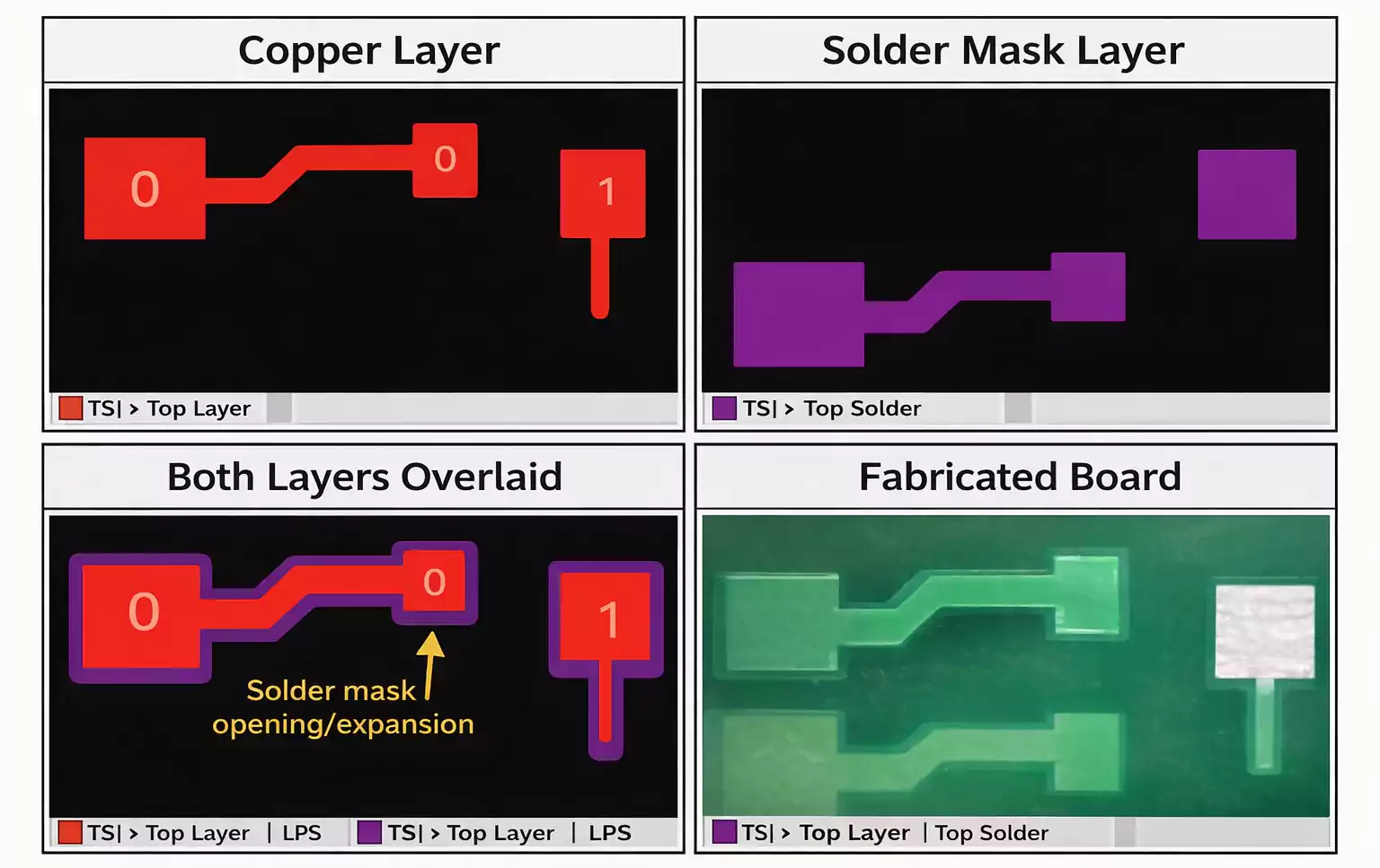
In PCB design, you’ll encounter several terms that often confuse new designers:
- Solder mask opening: The area where the mask is intentionally not applied so that pads or vias are exposed for soldering.
- Clearance: The minimum distance between the solder mask and copper features.
- Expansion: A deliberate adjustment to the opening size to compensate for manufacturing tolerances, misalignment, or to achieve specific pad definitions (such as NSMD vs SMD).
Balancing these parameters ensures that solder does not unintentionally migrate and that the mask doesn’t encroach on the copper pad, inhibiting solderability.
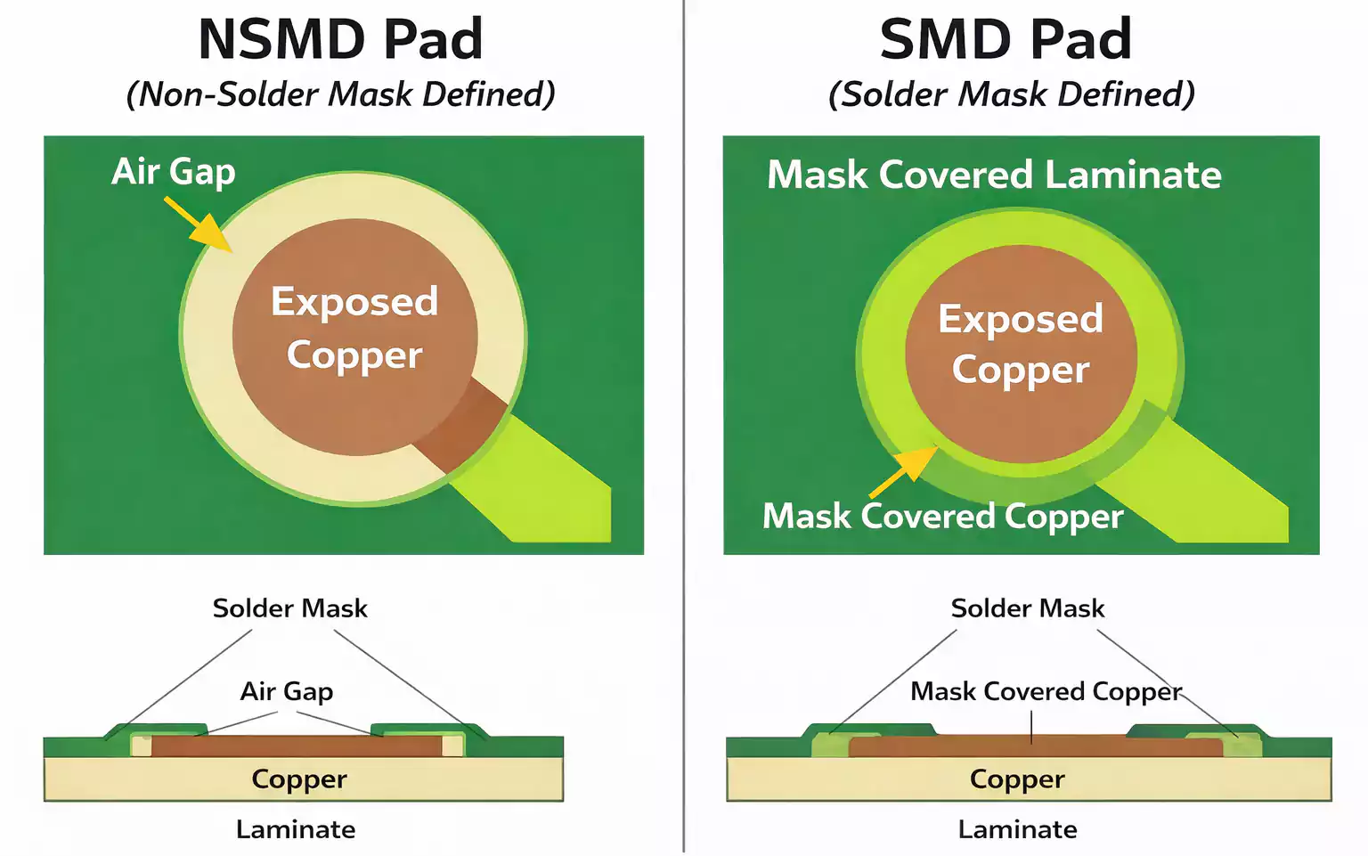
NSMD vs SMD Pads
Solder mask design influences pad type:
- NSMD (Non-Solder Mask Defined): The mask opening is slightly larger than the pad, allowing the solder to wet the copper fully. NSMD is common for fine-pitch BGAs and improves solder joint reliability.
- SMD (Solder Mask Defined): The mask opening is slightly smaller than the pad, so the solder mask edge overlaps the copper. This can provide mechanical support in constrained spaces but needs careful control to avoid interfering with solder wetting.
Properly configuring NSMD versus SMD pads in your CAD rules reduces assembly risks and prevents manufacturer beauty-sheet corrections.
Minimum Web and Silver Considerations
The mask “web” or sliver refers to narrow areas of solder mask between adjacent pads or traces. If mask expansion is too significant or pad spacing too tight, there might be insufficient mask material between features, increasing the risk of shorts. Proper mask dimensions must maintain a minimum web width (often specified by the PCB fabricator).
Practical DFM Rules
Good solder mask design adheres to standard practical rules, such as:
- Mask openings should generally be slightly larger than the copper pads to prevent accidental coverage.
- Maintain minimum clearance between the mask and traces to prevent unintended insulation failures.
- Consult your manufacturer’s capabilities before finalizing designs—mask tolerances and minimum web widths can vary with process technology.
Color and Aesthetics: Does It Matter?
While solder mask color does not affect electrical performance, it does have practical consequences:
- Green remains the default due to long-term use, good UV absorption characteristics during exposure, and strong contrast for inspection.
- Black-and-white boards are popular for aesthetic reasons but can make visual inspection more challenging.
- Other colors like red or blue might be used for revision control, prototyping differentiation, or branding.
In high-volume production, where inspection and yield are key, green is often the most practical choice.
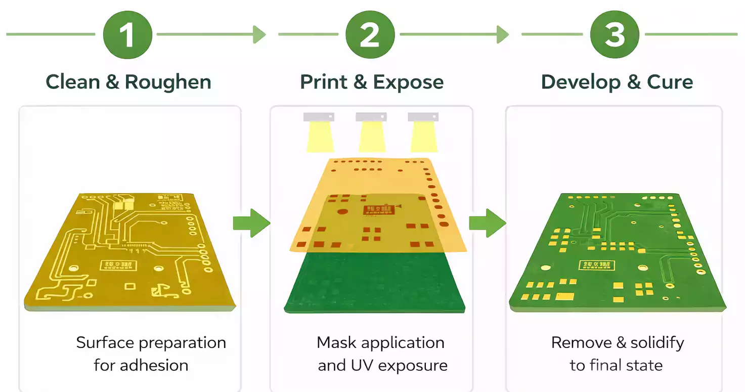
How Solder Mask Is Applied
The typical industrial solder mask application process involves these high-level steps:
- Panel preparation – copper surfaces are cleaned and roughened to improve adhesion.
- Coating – mask material is applied via curtain coating, screen printing, or spray.
- Pre-bake – a partial cure to stabilize the coating.
- Exposure and development – UV light defines openings according to photo masks.
- Final curing – fully crosslinks the mask for performance.
Dry-film or direct-print mask methods modify these steps but follow similar photolithographic principles.
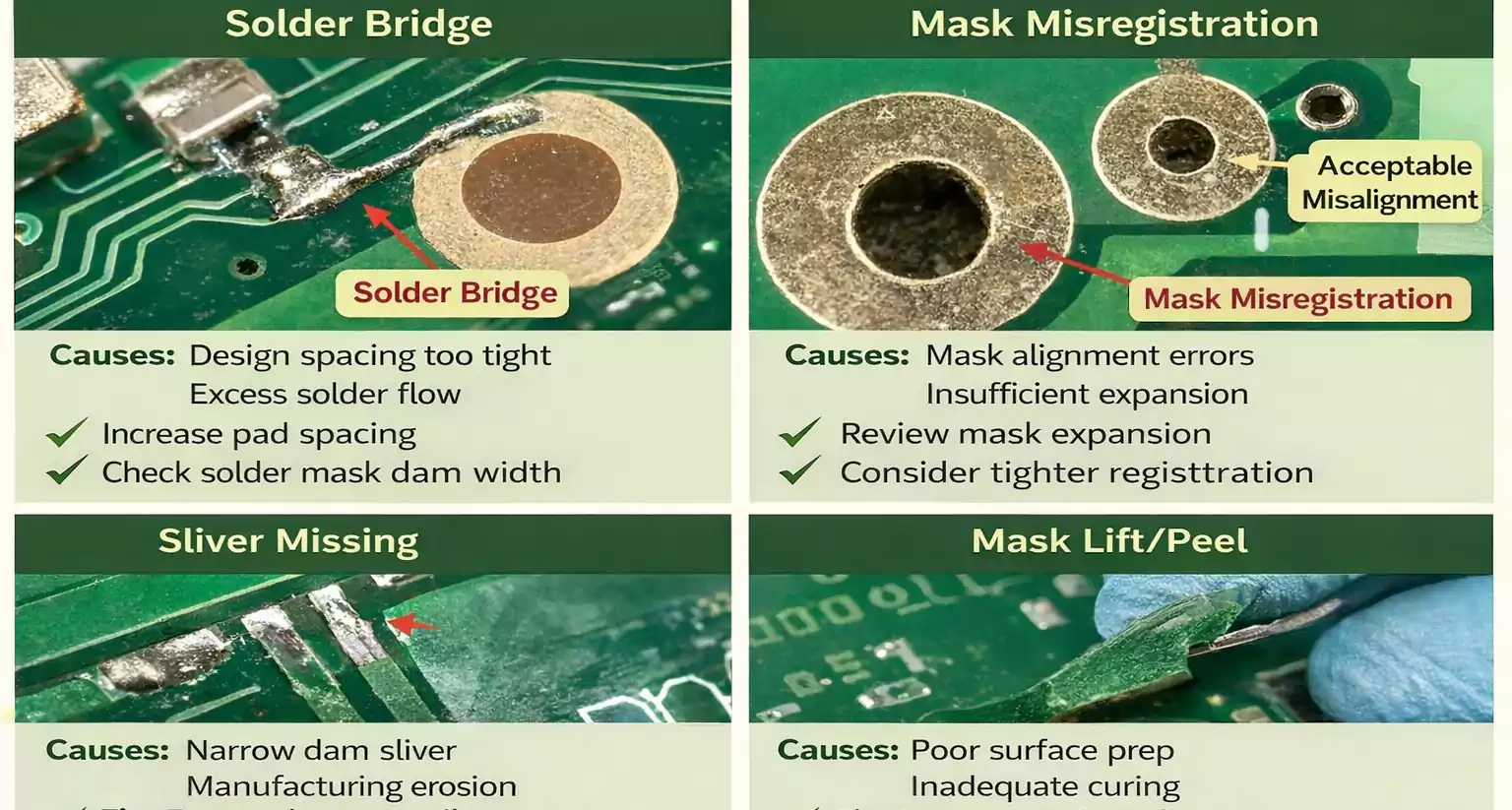
Common Solder Mask Issues and Troubleshooting
Even with good design, issues can crop up if manufacturing or assembly doesn’t go as expected.
Mask Misregistration
If the solder mask registration is off during fabrication, the mask may cover part of a pad or leave gaps, leading to poor solderability or weak joints. Proper expansion and clearance rules mitigate this.
Mask Slivers and Shorting
Too much expansion or too narrow spacing can eliminate the mask between pads, reducing its protective function and increasing the risk of solder bridging.
Contamination and Adhesion Failures
Improper cleaning or poor adhesion can cause mask lifting, bubbling, or peeling, exposing copper where it should be protected.
Temporary and Peelable Masks
In some assembly scenarios, a temporary or peelable solder mask is used to protect certain areas during soldering or rework. This is not a replacement for permanent solder mask—instead, it’s an assembly-specific protective layer that is removed after processing.
Communicating Solder Mask Requirements to Your Manufacturer
To avoid delays or unintended defaults in fabrication:
- Specify the pad type explicitly (NSMD vs SMD).
- Provide clear mask expansion/clearance values in the Gerber or in the fabrication notes.
- Confirm the minimum web/silver width based on your manufacturer’s DFM constraints.
- Clarify color, finish, and any peelable mask requirements upfront.
Quick FAQ
What’s the difference between solder mask and paste mask?
Solder mask is a permanent protective layer on the PCB that prevents shorts and corrosion, while a paste mask (stencil) is a temporary tool used to apply solder paste during assembly.
Is a solder mask required for every PCB?
For modern automated assembly (reflow or wave), yes—a mask is almost always required to ensure reliable solder joints. For simple hand-soldered boards, it is optional but still recommended.
How much expansion or clearance should I use?
There is no universal number—values vary with manufacturer capabilities, pad size, and pitch, but expansion in the 2–5 mil range is typical, coupled with enough mask web to prevent bridging.
Conclusion
The solder mask is much more than an aesthetic layer on a PCB—it is a critical protective and functional element that enables reliable manufacturing and long-term performance. By understanding what the solder mask does, how to design it properly, how it is applied, and how to troubleshoot common issues, you can dramatically improve product quality, yield, and reliability.
Getting the solder mask right requires good design decisions, careful DFM alignment, and clear communication with your PCB fabricator. With the proper foundation, your PCBs will last.
