

In electronic system design, a PCB is not an isolated “board.” It’s one layer in a broader electronic packaging system. To understand what a PCB really does—and why certain board types and assembly methods are chosen—you need to look at the problem through packaging levels (packaging hierarchy). Each level maps to different manufacturing processes, reliability risks, cost drivers, and performance constraints.
This article explains the Level 1–Level 3 packaging model and clarifies the PCB’s role, boundaries, and key engineering tradeoffs.
Factors That Influence Electronic Packaging Choices
Electronic packaging options are wide-ranging. Engineers typically weigh:
- Quality & reliability (lifetime, failure mechanisms, field conditions)
- Size & volume (form factor, Z-height, density)
- Cost (materials, assembly, yield, test, rework)
- Electrical performance/speed (signal integrity, power integrity, EMI/EMC)
- Manufacturability (process maturity, yield, throughput, supplier capability)
- Repairability (rework feasibility, access, inspection)
- Function & environment (temperature, humidity, shock, vibration, chemicals)
A helpful way to summarize packaging goals—regardless of level—is:
Electrical interconnection + thermal management + mechanical/environmental protection
There’s no universally “best” packaging approach—only what best fits your product requirements and supply chain reality.on.
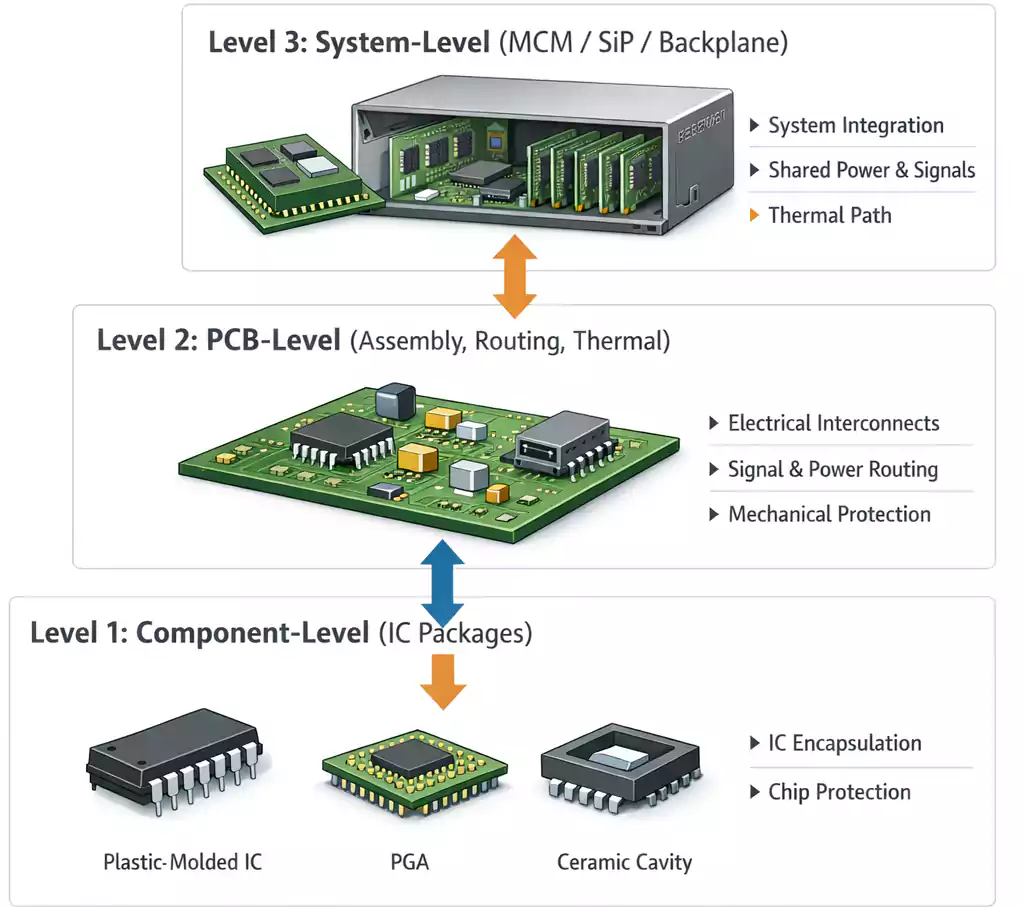
Packaging Levels: A Practical Way to Break Down Complexity
Your original content uses a very practical three-level model:
- Level 1: Component-level packaging (single device package)
- Level 2: Board-level packaging (components assembled onto a PCB/substrate)
- Level 3: System-level packaging (modules and assemblies beyond a single PCB)
Some industry references subdivide further (chip-level, wafer-level, etc.), but Level 1–3 is clear and highly usable for design and manufacturing discussions—so we’ll stick with it.
Level 1 Packaging (Component-Level Packaging)
Definition:
Level 1 packaging refers to the housing and interface of an individual component—especially ICs—so the silicon die becomes a usable part that can be handled, assembled, and connected to higher-level interconnect.
Typical forms include:
- Plastic packages (molded packages)
- Cavity (hermetic or non-hermetic) packages
- Pin Grid Array (PGA)
Core functions:
- Protect the die from contamination, moisture, and mechanical damage
- Provide a standardized external interface (leads, balls, pads, pins)
- Provide mechanical support and a partial thermal path for heat removal
Why there are so many package styles:
Component packaging must balance I/O count, pitch, thermal performance, mechanical robustness, and cost. That’s why you see a large variety of standardized package families—and why PCB footprint (land pattern) accuracy is fundamental to manufacturability.
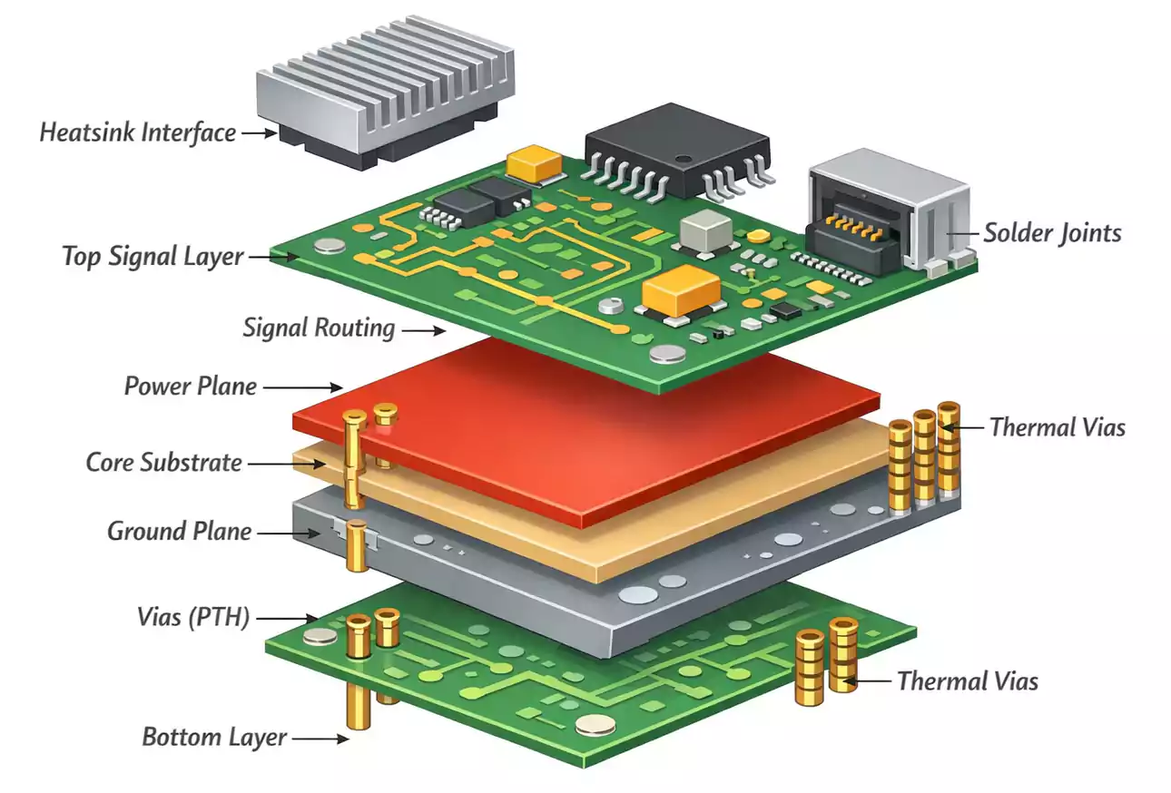
Level 2 Packaging (Board-Level Packaging): Where PCBA Happens
Definition:
Level 2 packaging is the assembly of components onto a PCB or substrate to form a functioning circuit—often referred to in production terms as PCBA (Printed Circuit Board Assembly).
What it includes:
- Component attachment and soldering (SMT, through-hole, mixed technology)
- Electrical interconnect on the board (traces, planes, vias)
- Mechanical retention and basic thermal design (copper areas, layout, mounting, TIMs where needed)
Level 2 in “manufacturing language”:
In industry, Level 2 is strongly associated with SMT/assembly processes. The key question becomes:
“Can we reliably assemble, inspect, test, and (if needed) rework this design at acceptable yield and cost?”
How component packaging shows up at Level 2:
All component packages ultimately translate into PCB footprints (land patterns)—pad shape, pitch, solder mask rules, paste apertures, and assembly windows. Packages like QFN, BGA, and fine-pitch leaded devices have very different assembly sensitivities. In other words, Level 1 choices directly constrain Level 2 manufacturability.
Common Level 2 carriers include:
- Single-sided / double-sided PCBs
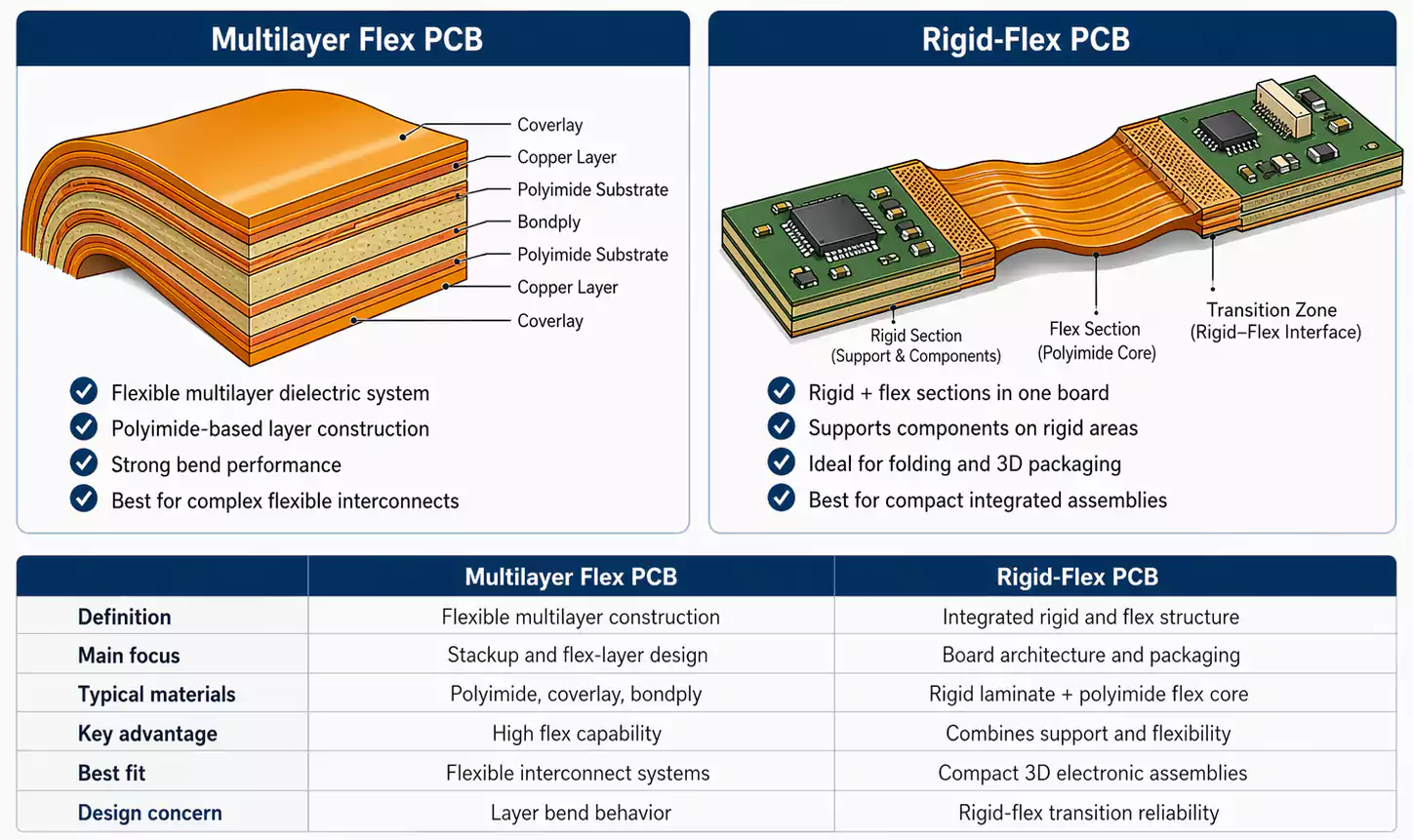
- Multilayer PCBs
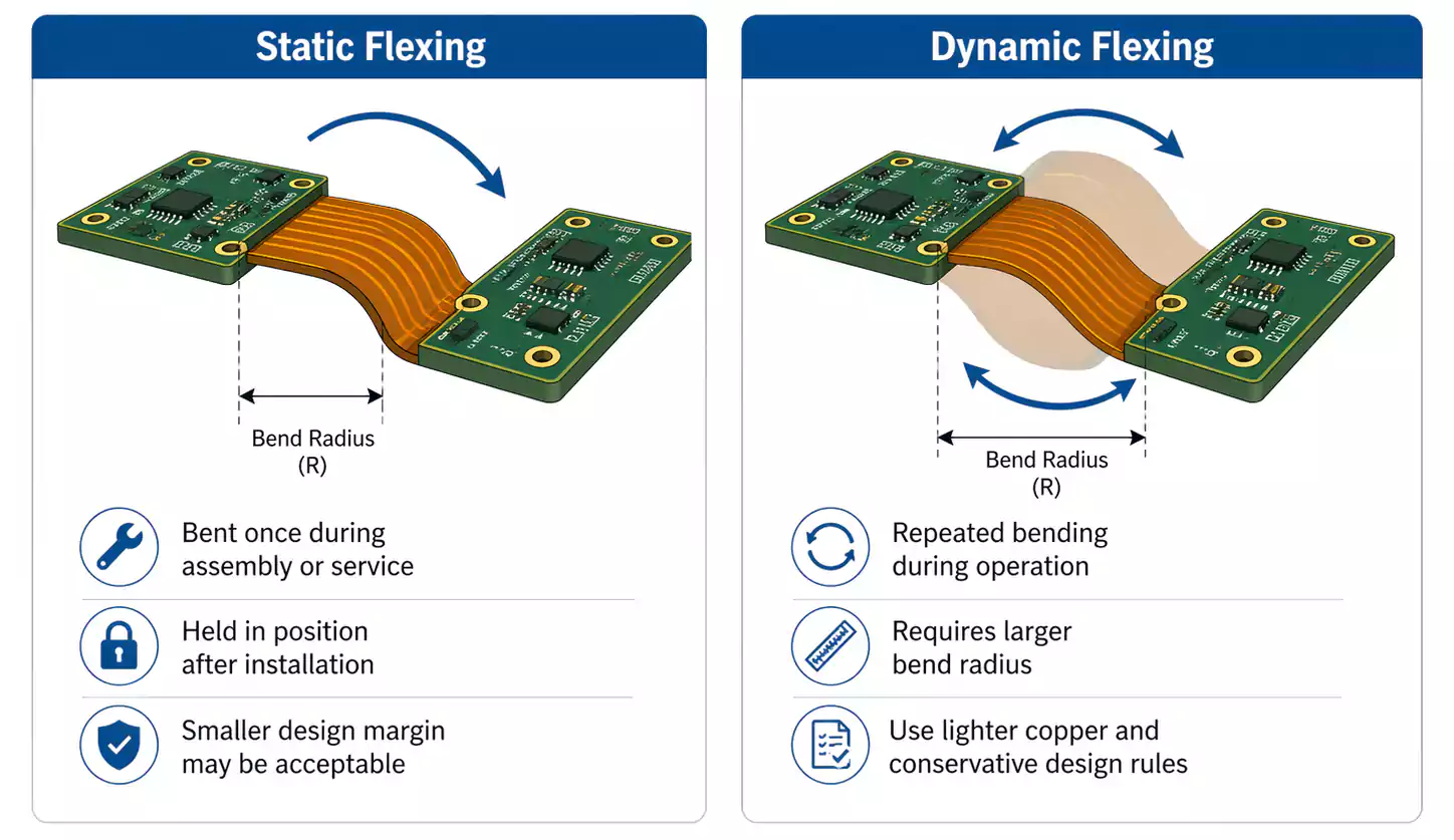
- Flexible PCBs (FPC)
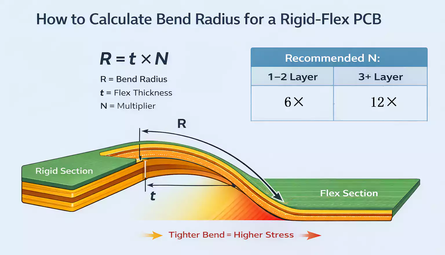
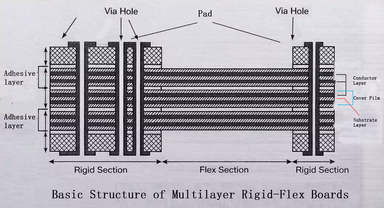
- Rigid-flex PCBs
For most electronic products, Level 2 is the core packaging layer where performance, cost, and reliability intersect.
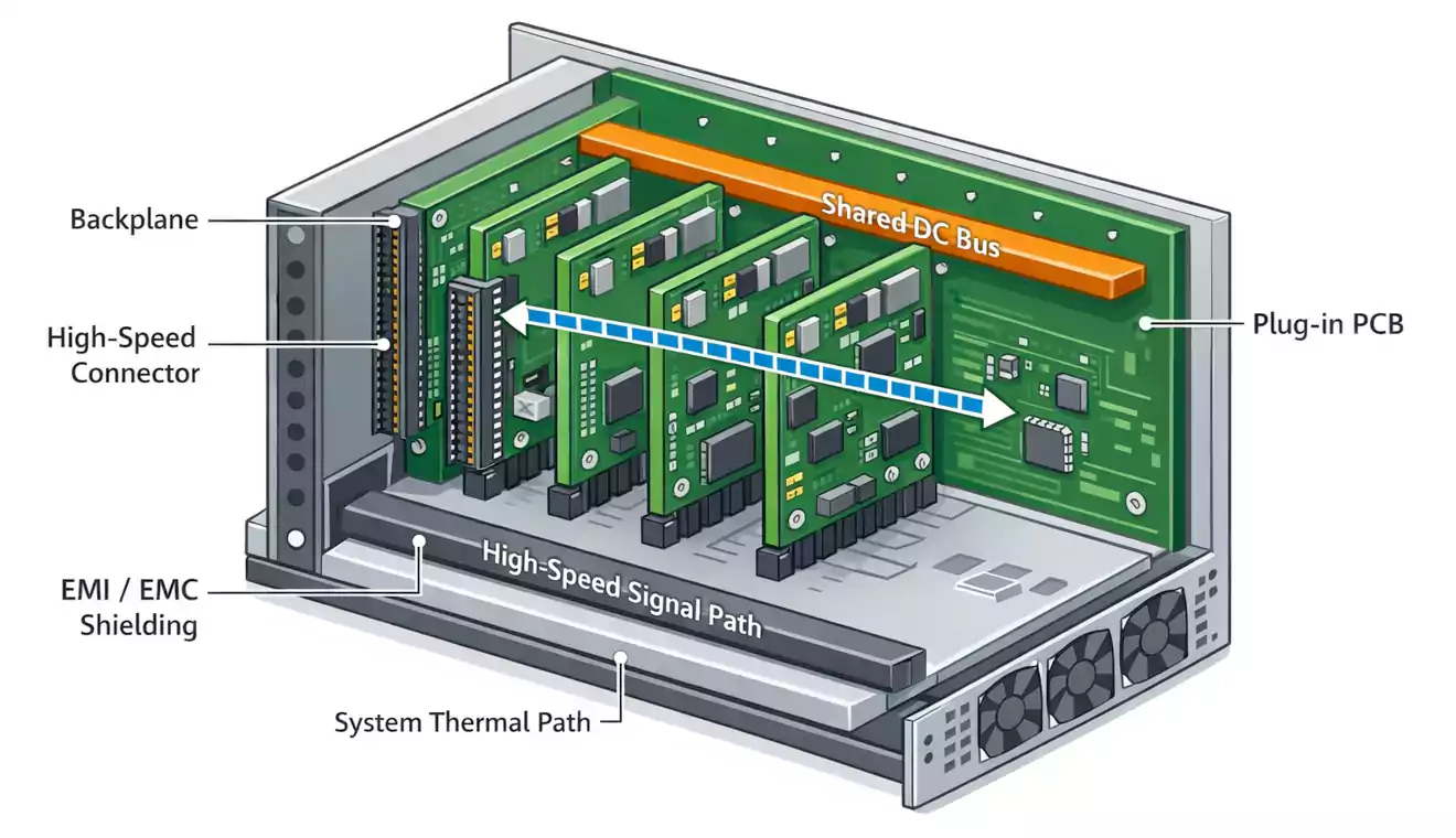
Level 3 Packaging (System-Level Packaging): Modules and Assemblies Beyond One Board
Definition:
Level 3 packaging refers to packaging forms beyond a single PCB—assembling one or more PCBAs along with connectors, cables/harnesses, shields, heat sinks, chassis structures, and other mechanical elements into a module or subsystem, and ultimately into a complete product.
Typical forms include:
- Multi-Chip Modules (MCMs)
- Modular system packaging (cards, sub-assemblies, multi-board stacks, enclosures)
Key characteristics:
- Integrates multiple chips or sub-modules working together
- Optimizes at the system level: size, reliability, performance, serviceability
- Brings in strong mechanical, thermal, and EMI/EMC considerations
A helpful way to think about it:
Level 3: “How do boards become a reliable module/system in the real world?”ponents or modules onto a printed circuit board (PCB) or substrate to form a complete electrical circuit.
Level 1: “How does silicon become a usable component?”
Level 2: “How do components become a reliable assembled board (PCBA)?”
Relationship Between Packaging Levels and PCBs
| Level 1 | Single component | IC packages, PGA |
| Level 2 | Circuit assembly | PCB with mounted components |
| Level 3 | System integration | MCM, backplanes, complete modules |
The PCB serves as the bridge between Level 1 and Level 3 packaging, linking individual electronic packages into a unified, functional system.
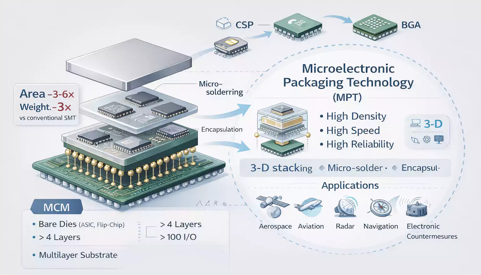
Why MCM Is Often the “Representative” Level 3 Example
What is an MCM?
A Multi-Chip Module (MCM) integrates multiple ICs (sometimes bare die) and/or discrete components onto a single module substrate, presenting itself externally as a single functional block—often like a “bigger IC.”
Common implementation notes:
- The module substrate can be laminated (PCB-like), ceramic, or thin-film, depending on interconnect density, thermal needs, and reliability requirements.
- MCMs may use advanced interconnect methods such as flip-chip to increase I/O density and reduce parasitics.
Why use MCM?
- Enables heterogeneous integration (mixing different technologies)
- Can improve overall yield vs. one huge monolithic die
- Supports modular system design and performance/cost optimization at the subsystem level
IC Substrate vs. PCB: Where’s the Boundary?
A common confusion is treating IC substrates (package substrates) and PCBs as the same thing. A practical distinction is:
- IC substrate is “chip-centered.” It lives inside (or very close to) the component/module packaging and serves as a high-density transition between silicon and the outside world.
- PCB is “system-centered.” It connects many components and forms the functional platform for the product.
A useful mental model:
A substrate is often like a high-density “mini board” inside a package, while a PCB is the primary electrical platform for the whole system.
This distinction helps clarify packaging levels:
PCBs/PCBAs most commonly map to Level 2.
Substrates can sit between Level 1 and Level 3 depending on how they’re used (inside a package, inside an MCM, etc.).
FAQ — Electronic Packaging
What is electronic packaging?
Electronic packaging is the mechanical, electrical, and thermal framework that protects components, routes signals/power, and enables reliable assembly from chip to system.
What are the three levels of electronic packaging?
Level 1: the component/package (single device).
Level 2: the PCB-level assembly of multiple electronic packages.
Level 3: system-level integration (multiple boards/modules).
How do PCBs fit into electronic packaging?
The PCB is the Level-2 carrier that supports electronic packages and interconnects them, bridging chips (Level-1) to systems (Level-3).
How do multilayer PCBs help?
They add power/ground planes and controlled-impedance routing to improve signal integrity, power integrity, and EMI performance.
When should I use rigid-flex?
Use rigid-flex for compact 3D folding, fewer connectors/cables, higher reliability, and weight/space savings.
What is a backplane at Level-3?
A backplane is a slot-based PCB that ties multiple boards into one system and distributes power/high-speed signals.
How does electronic packaging manage heat?
By providing conductive paths, thermal pads/spreaders, and suitable interface materials to keep junction temperatures within spec.
Conclusion
From single-chip electronic packages to multi-board systems, electronic packaging represents the art and science of balancing performance, space, and manufacturability.
Understanding these packaging levels helps engineers choose the right PCB technologies and assembly methods to achieve optimal reliability and performance.
In essence, electronic packaging is where physics, materials, and manufacturing converge — turning electronic concepts into real, functional products.
