

When you see the term chip on board (COB) online, it can mean two different things.
In electronics manufacturing, COB is a packaging method that mounts bare semiconductor dies directly on a printed circuit board (PCB).
In lighting, a COB LED is a high-density LED module in which many LED chips are mounted closely together on a substrate.
This guide explains both meanings — how COB packaging works, how to design PCBs for it, and why COB LEDs and LED strips are becoming so popular in lighting and display products.
What Is Chip on Board (COB)?
In simple terms, chip on board means a bare silicon die is attached directly to the PCB rather than enclosed in a plastic IC package.
After the chip is attached, tiny gold or aluminum wires connect the die pads to copper pads on the board.
Finally, a protective epoxy layer called a glob top covers the area to protect it from moisture, dust, and mechanical stress.
By removing the traditional plastic package, COB reduces size, cost, and electrical parasitics. It is often called a “level-1.5 packaging” technology — halfway between chip-level and board-level assembly.
COB Structure and Key Components
A typical COB assembly includes:
- Bare die: the unpackaged silicon chip.
- Bond pads: tiny metal areas on the die used for wire connections.
- Die attach adhesive: conductive or non-conductive glue used to secure the die.
- Wire bonds: thin gold or aluminum wires that connect die pads to PCB pads.
- Encapsulation (glob top): an epoxy or silicone layer that seals and protects the wires and die.
This structure keeps the signal path short, thereby improving electrical performance and heat transfer.
Two Main Connection Styles: Wire Bonding vs. Flip Chip
There are two common ways to connect a die to the PCB in COB designs.
1. Wire Bonding
This is the classic approach. The die is glued face-up, and thin wires connect each pad on the die to matching pads on the PCB.
Wire bonding is flexible and inexpensive, but it adds some height and length to the electrical path.
2. Flip Chip on Board
Here, the die is flipped face down and solder-bumped directly to the PCB pads.
It eliminates the bonding wires and makes the path even shorter — great for high-frequency or high-current designs — but requires tighter alignment and a cleaner process.
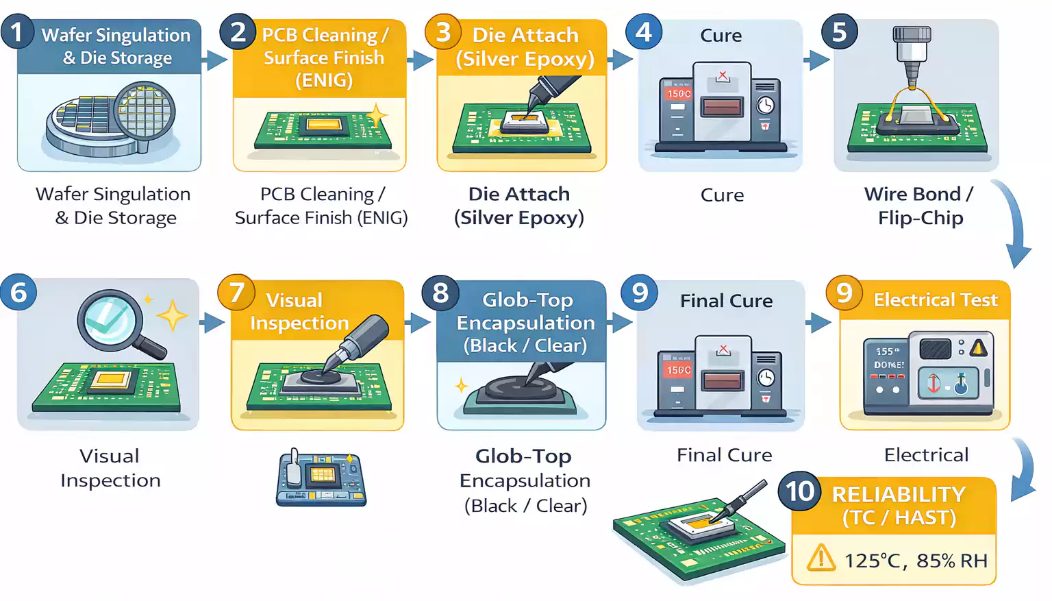
How a Chip on Board Assembly Is Made
The manufacturing process is more precise than standard surface-mount assembly.
Here’s the typical sequence:
- Die preparation and storage: Bare chips are diced from the wafer and stored in dry, clean containers to prevent oxidation.
- Board cleaning: The PCB surface must be spotless and flat. Any oil or dust can cause poor bonding.
- Die attach: A small drop of adhesive (often silver epoxy) is placed on the pad, and the die is positioned and cured.
- Wire bonding: The wire bonder connects die pads to PCB pads using ultrasonic or thermosonic bonding.
- Encapsulation (glob top): Epoxy is dispensed to cover the die and wires. Black epoxy blocks light and protects from UV; clear epoxy allows inspection.
- Curing: The board is heated to harden the epoxy.
- Testing and inspection: Visual checks, continuity tests, and sometimes X-ray or electrical testing ensure good connections.
- Reliability testing: Thermal cycling and humidity stress tests verify long-term stability.
The process requires controlled temperature, humidity, and cleanliness — and once completed, the part is almost impossible to rework.
Advantages and Limitations of COB Packaging
Advantages
- Smaller size and lower cost: No plastic package or lead frame needed.
- Better electrical performance: Shorter connection path reduces resistance and inductance.
- Improved thermal path: The die can dissipate heat directly through the board.
- Flexible design: Multiple chips (MCU, sensor, memory) can share one board area.
Limitations
- Difficult to rework: Once encapsulated, it is difficult to repair.
- Requires cleanroom process: Dust or oxidation can cause open bonds.
- Sensitive to moisture and stress: Poor encapsulation can cause failures.
For these reasons, COB is common in low-cost consumer electronics, sensors, and custom modules, but is less used in high-reliability products like automotive ECUs or medical devices.
Design Tips for a Reliable COB PCB
To make Chip on Board manufacturing successful, PCB designers need to consider several layout and material details.
1. Surface Finish
Wire bonding requires a smooth, bondable surface.
ENIG (Electroless Nickel Immersion Gold) or electroplated hard gold finishes are preferred because they provide consistent adhesion for gold or aluminum wires.
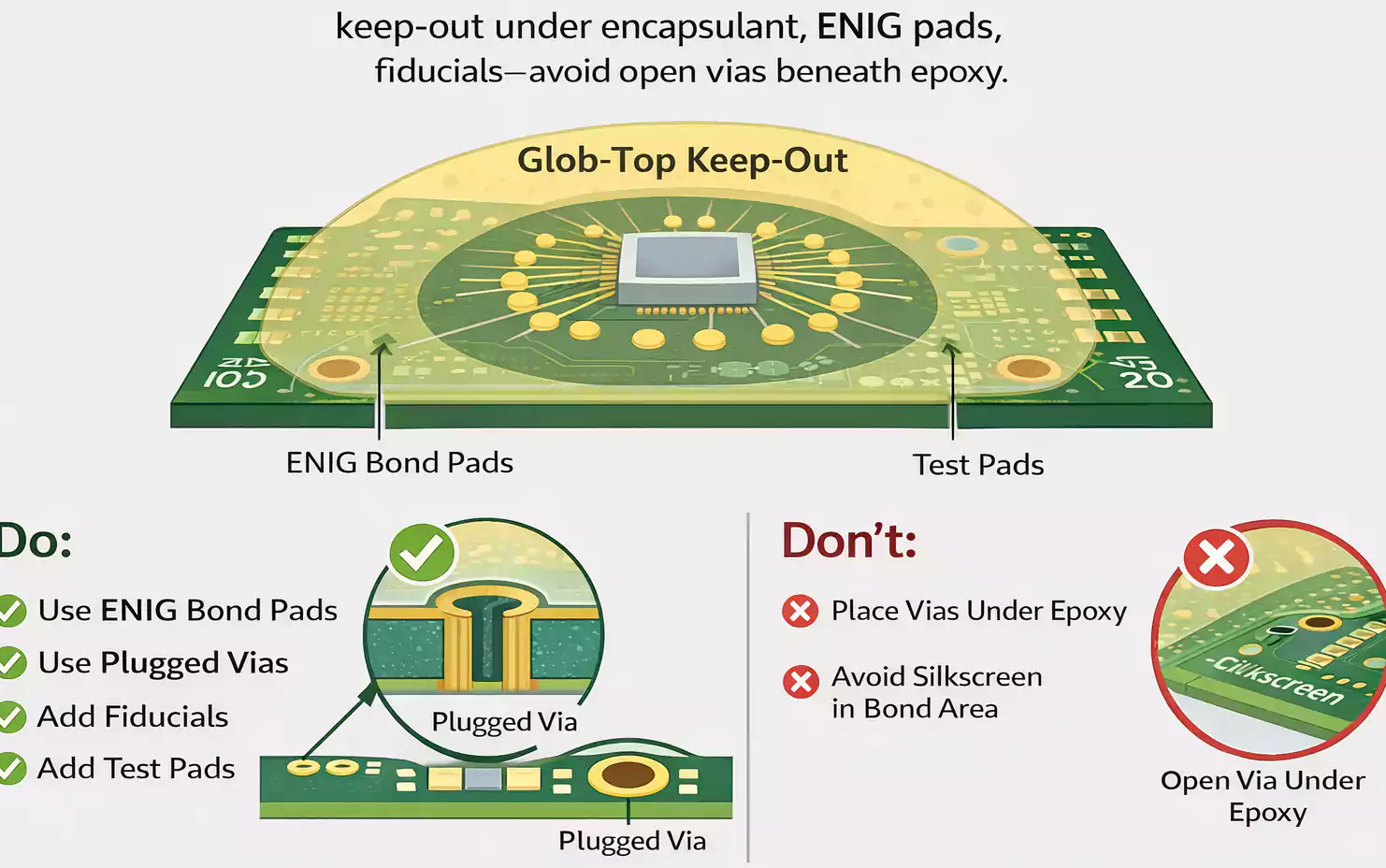
2. Keep-Out Zones for Encapsulation
The glob top epoxy flows during curing.
Avoid placing vias or copper features under the epoxy region.
If vias are required, they must be filled or plugged to prevent resin leakage or air bubbles.
3. Pad Design for Wire Bonding
Bond pads must be large enough for the bonding capillary to land safely but spaced to prevent shorting.
Follow your bonding house’s minimum pad size and spacing rules.
4. Thermal Design
Plan a direct heat path from the die to copper or metal layers below.
For high-power ICs, use thermal vias or metal cores to dissipate heat away from the die.
5. Assembly Alignment and Markings
Add fiducials and reference marks to help automatic bonding machines align the die correctly.
Avoid silkscreen or solder mask in the bonding and encapsulation zones.
Common COB Defects and How to Avoid Them
| Broken wire bonds | Poor adhesion, contamination | Clean PCB, proper surface finish |
| Lifted pads | Stress during bonding | Optimize bonding force and temperature |
| Air bubbles or voids | Poor epoxy dispensing | Controlled flow and degassed material |
| Corrosion or shorting | Moisture under glob top | Use moisture-resistant encapsulant, bake before encapsulation |
| Delamination | Thermal mismatch | Match CTE between board and epoxy |
Because COB assemblies are not reworkable, reasonable process control and inspection are essential before encapsulation.
Applications of COB Packaging
- LED modules – many LED manufacturers mount bare dies on aluminum substrates.
- Low-cost toys and gadgets – common in “black-blob” ICs on cheap PCBs.
- Custom sensors and ASIC prototypes – small batches where no standard package exists.
- Compact IoT or RF modules – short connections for better signal integrity.
What Is a COB LED?
In lighting, Chip on Board refers to the same principle — multiple LED chips mounted directly on a thermally efficient substrate.
Instead of packaging each LED individually (like SMD), dozens or even hundreds of tiny LED dies are placed very close together and covered with a single layer of phosphor and silicone.
This creates a uniform, bright light surface that behaves like a single powerful emitter.
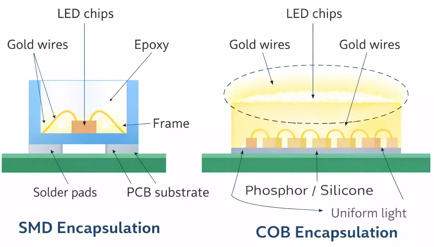
Because the light-emitting area is continuous, COB LEDs deliver higher lumen density and better color uniformity compared to SMD arrays.
COB LED vs. SMD LED
| Structure | Many chips on one substrate, single phosphor layer | Each LED packaged separately |
| Light uniformity | Continuous, no visible dots | Visible points, needs diffuser |
| Thermal performance | Better – heat spreads over large metal area | Moderate – each LED has its own pad |
| Ease of assembly | Fewer solder joints | Many solder joints |
| Applications | Downlights, floodlights, displays, LED strips | General lighting, indicator boards |
For LED displays, COB technology allows a smaller pixel pitch and a flatter, more durable surface than traditional SMD modules.
For lighting, COB LEDs simplify optical design and increase luminous efficiency.
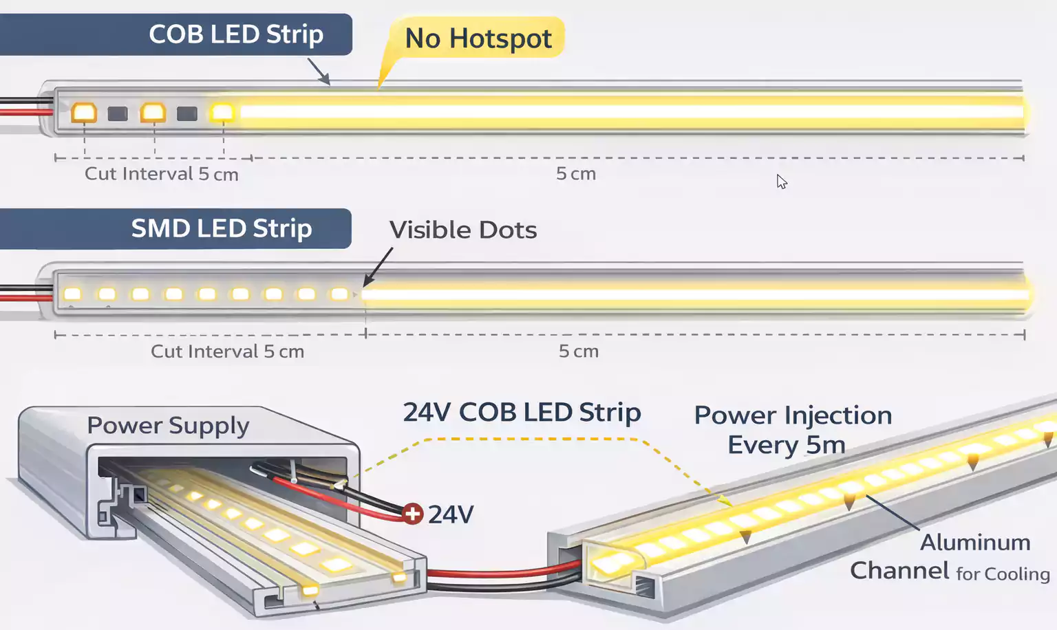
COB LED Strips: Uniform Light with No Hotspots
A COB LED strip is an LED tape that uses the same concept — many tiny LED dies placed close together under a continuous phosphor coating.
Unlike standard SMD strips, you won’t see individual dots of light.
The output looks like one smooth, seamless line of light.
Advantages
- No dark spots or “dot effect.”
- More flexible light diffusion without extra covers.
- Slim and bendable, perfect for cabinets, shelves, or decorative lines.
- Available in 12V and 24V versions for easy installation.
Limitations
- Slightly more expensive per meter.
- Needs good heat dissipation — mounting on aluminum channels is recommended.
- Harder to repair individual sections.
How to Choose a COB LED Strip
When shopping for or designing with COB LED strips, consider these parameters:
- Voltage:
12V strips have shorter cut intervals but greater voltage drop; 24V strips handle more extended runs. - Power and brightness:
Rated in watts per meter and lumens per meter. Match to your desired brightness and power supply. - Color temperature and CRI:
A high CRI (≥90) provides better color rendering. Choose 2700K–6500K depending on the ambience. - LED density:
Typical COB strips range from 320 to 640 chips per meter — more chips mean smoother light. - Protection and environment:
For outdoor or humid areas, select IP65–IP67 coated versions. Be aware that thick silicone can yellow over time. - Dimming compatibility:
Check if your power supply and controller support PWM or analog dimming.
Heat Management and Lifespan
Just like any LED, COB LEDs and strips generate heat.
If the LED junction temperature rises too high, light output drops and color shifts.
To extend lifespan:
- Mount COB strips on aluminum channels or metal surfaces.
- Ensure good airflow and avoid enclosed spaces.
- Use power supplies with adequate current margin.
A well-cooled COB strip can last 30,000–50,000 hours with minimal brightness decay.
FAQ
What does chip on board mean?
It’s a packaging technique that attaches bare chips directly to a circuit board and protects them with epoxy.
Is COB the same as flip chip?
Flip chip is one implementation of COB where the die is flipped and soldered face down.
Why is COB cheaper?
It removes the need for a molded plastic package and lead frame.
What is a COB LED?
A light source made by mounting multiple LED dies closely together on a substrate for higher brightness and uniformity.
COB vs. SMD LED strip — which is better?
COB gives smoother light with no dots; SMD is cheaper and easier to repair.
Do COB LED strips need aluminum channels?
Yes, for high-power or long runs, aluminum helps dissipate heat and extend lifespan.
Conclusion
Whether you’re designing a custom PCB with bare dies or choosing the latest seamless LED strips, Chip on Board technology offers compact size, high performance, and improved reliability.
In electronics, COB enables smaller, cheaper assemblies by eliminating traditional IC packages.
In lighting, it delivers brighter, smoother, and more efficient illumination.
Understanding how COB works — from bonding wires and encapsulation to LED density and heat management — helps engineers, makers, and lighting designers create products that are both efficient and durable.
