

When you search "pad thermal," you’ll find results about thermal interface materials, IC package pads, and PCB design techniques. The confusion is natural—"thermal pad" means different things in various engineering contexts.
This article clarifies the term. Whether you’re choosing between thermal pads and paste, working with exposed thermal pads on ICs, or managing solderability on ground-plane pads, we’ll guide you to the right choice.
Thermal Pads as Thermal Interface Materials (TIMs)
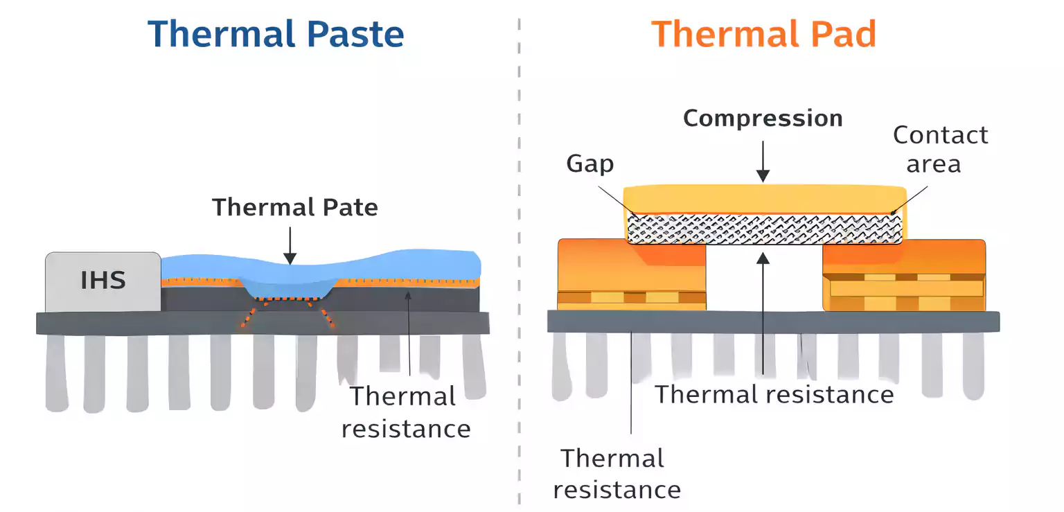
A pad thermal is a soft, thermally conductive material placed between a heat-generating component and a heatsink or chassis.
Its purpose is simple: fill microscopic air gaps and improve surface contact, allowing heat to flow efficiently from the component to the cooling surface.
Air is a poor conductor of heat. Even smooth surfaces have imperfections that trap air, increasing thermal resistance.
A thermal pad deforms slightly under pressure, replacing air with a material that conducts heat much better — creating a consistent, reliable thermal path.
Common Applications
- CPUs, GPUs, and VRMs
- Power regulators and converters
- LED modules and lighting drivers
- Automotive control units
- Industrial and telecom power electronics
Common Types of Thermal Pads
Silicone Pads – The most common type, combining flexibility, electrical insulation, and decent thermal performance.
Graphite or Carbon Pads – Thinner and highly conductive, but require flat, clean surfaces. Typically not electrically insulating.
Silicone-Free Pads – Used in optical, sensor, or medical systems where silicone outgassing can cause contamination.
Key Pad Thermal Specifications
Understanding datasheet specs helps you select the right pad for your design — and avoid costly overheating issues.
1. Thermal Conductivity (W/m·K)
This indicates how efficiently a material conducts heat.
A higher value is better, but real performance depends on surface flatness, compression, and contact pressure.
In practice, a well-fitted 5 W/m·K pad can outperform a poorly installed 10 W/m·K pad.
2. Thickness vs. Gap
A common mistake: thinking thicker pads always perform better.
In reality, thicker pads introduce more internal thermal resistance.
Choose the thinnest pad that still fills your mechanical gap with slight compression — typically 10–20% thicker than the measured clearance.
3. Hardness and Compressibility
Softer pads conform better to uneven surfaces but may deform under pressure.
Harder pads maintain shape but require smoother, flatter surfaces.
Select medium hardness (Shore 00 40–60) for general use.
4. Electrical Insulation and Temperature Range
If the pad sits between conductive parts, check dielectric strength (usually > 3 kV/mm).
Also, verify the operating temperature — especially in automotive or power designs where 125–150 °C operation is common.
Thermal Pad vs Thermal Paste: Which Is Better?
Both pad thermal and thermal paste improve heat transfer between a device and a heatsink — but they behave differently in performance, consistency, and maintenance.
1. Quick Comparison
| Ease of Application | Pre-cut, clean | Requires careful spreading |
| Gap-Filling Ability | Moderate to high | Low (only for flat, small gaps) |
| Consistency | Very consistent | Depends on user/application |
| Reusability | Often reusable | Must be cleaned and reapplied |
| Electrical Insulation | Usually insulating | Usually not insulating |
| Thermal Performance | Slightly higher resistance | Lower resistance (best for CPUs) |
| Maintenance | Simple | Messy, time-consuming |
2. Are Thermal Pads Better Than Paste?
That depends on your setup.
Use thermal pads when:
- You have uneven surfaces or large gaps.
- Electrical insulation is required.
- The design needs repeatable, clean assembly.
- You value long-term stability (pads don’t dry or pump out)
Use thermal paste when:
- The surfaces are very flat and close.
- You need maximum thermal conductivity.
- You can manage precise application and maintenance.
Pad Thermal is cleaner, more consistent, and better for production. Paste performs slightly better for peak cooling when conditions are ideal.
3. Common Mistakes
- Choosing pads that are too thick (increases thermal resistance)
- Not applying enough pressure to ensure contact.
- Confusing thermal pad, adhesive pad, and double-sided tape
- Using paste where a pad fits better (like on VRAM or power ICs)
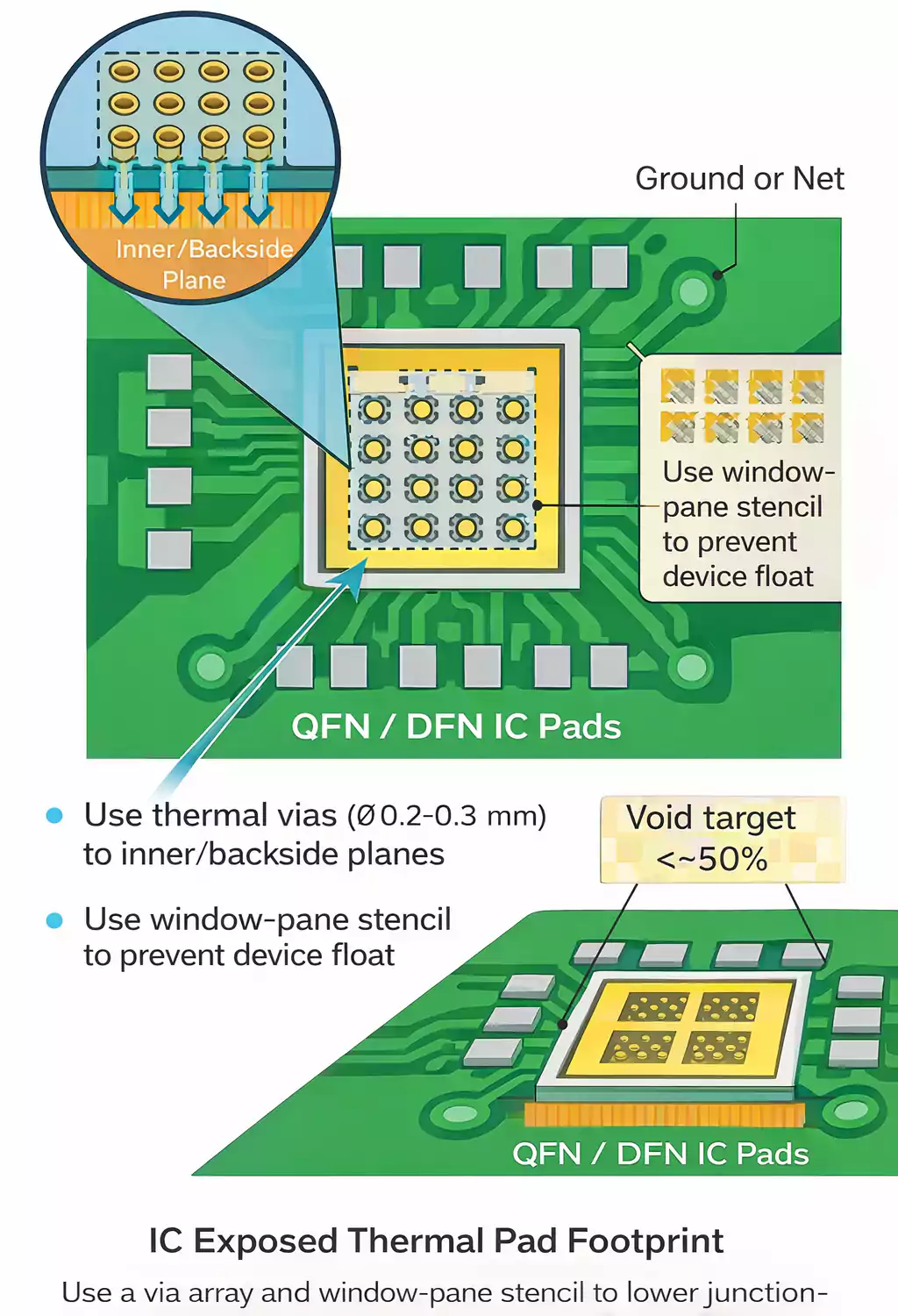
IC Package Thermal Pads (Exposed Pads)
Many surface-mount ICs, such as QFN or DFN packages, include a large metal pad on the bottom known as an exposed pad thermal or die pad.
This pad must be soldered to the PCB to ensure proper heat dissipation and mechanical stability.
1. Why It Matters
The exposed pad creates a low-resistance thermal path from the silicon die to the PCB copper plane.
If it’s not soldered, air gaps form — reducing heat transfer and potentially causing device failure or thermal drift.
Datasheet thermal resistance values always assume this pad is properly soldered.
2. Electrical Connection
Check the IC datasheet carefully.
Most exposed pads connect to ground, but some may be tied to another potential or left floating. Never assume — misconnection can cause shorts or EMI problems.
3. PCB Design Tips
- Pad Size: Match the PCB land to the package pad size.
- Thermal Vias: Use small vias (0.3 mm or less) under the pad to move heat to internal or bottom layers.
- Stencil Design: Don’t flood the pad with paste; use a windowpane pattern to prevent paste from floating during reflow.
- Void Control: Limit solder voids (ideally < 50%) to ensure good thermal contact.
A properly soldered exposed pad can halve the junction-to-board thermal resistance.
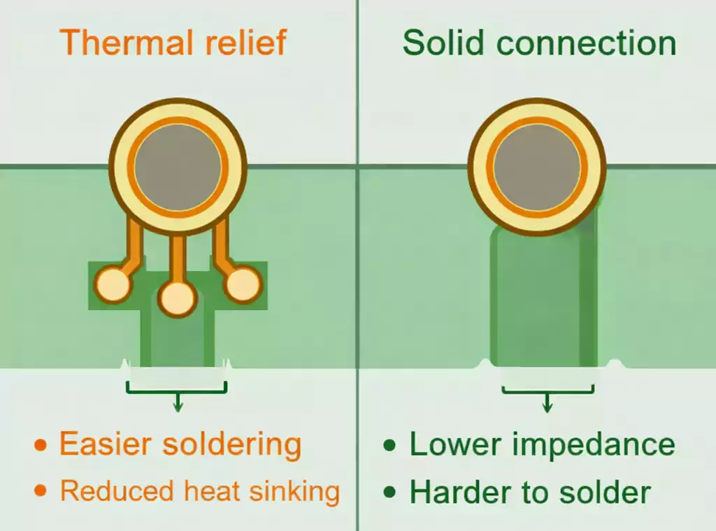
PCB Thermal Relief Pads
In PCB manufacturing, large copper pours (like ground planes) can make soldering difficult.
Pads directly tied to these planes absorb heat during reflow, preventing solder from melting evenly.
A thermal relief pad addresses this by connecting to the plane via narrow spokes.
1. How It Works
The spokes reduce heat conduction into the plane during soldering, allowing the pad to reach reflow temperature faster.
After soldering, they still provide good electrical and thermal connection — just not as strong as a solid tie.
2. When to Use
- Through-hole pads connected to ground or power planes
- Boards assembled via wave soldering or manual soldering
- To prevent cold joints, tombstoning, or uneven heating
3. When Not to Use
- High-current or low-impedance paths (can add unwanted resistance)
- RF circuits where spoke inductance affects performance.
- Power devices that rely on solid copper for heat dissipation
FAQ
Are thermal pads better than thermal paste?
Pads are better for assembly consistency and insulation. Paste gives slightly better cooling when surfaces are perfectly flat.
Can thermal pads be reused?
Sometimes, if they stay intact. For consistent results, replacement is recommended during reassembly.
What is an IC thermal pad?
It’s the exposed metal pad under some ICs (like QFNs) that must be soldered to the PCB for heat transfer — and sometimes grounding.
What is a thermal relief pad in PCB design?
A pad connected to a plane through narrow copper spokes, designed to make soldering easier by slowing heat flow.
Why is it hard to solder pads tied to a ground plane?
The copper plane acts as a heat sink, pulling heat away. Thermal relief pads help maintain soldering temperature.
Final Thoughts
“Pad thermal” is one term with multiple meanings —
- Thermal interface pads manage heat between devices and heatsinks,
- IC exposed pads transfer heat from the die to the PCB,
- PCB thermal relief pads make soldering large copper connections reliable.
Understanding these differences helps you design for better thermal performance and manufacturability.
If you’re developing a PCB that requires precise thermal control, FastTurnPCB provides DFM reviews, exposed pad layout optimisation, and manufacturing solutions to ensure reliable thermal and solder performance.
