

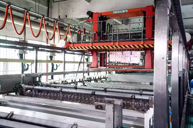
Electroless copper plating is a crucial process for hole metallization in PCB manufacturing and is widely used in the electronics industry, especially for the production of high-density, multi-layer PCBs. Its main purpose is to deposit a uniform copper layer on the walls and surface of PCB holes to ensure reliable electrical connections and signal transmission.
This article provides a detailed analysis of the electroless copper plating process and its underlying mechanisms, helping readers better understand this important process.
Process Overview
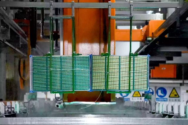
After drilling and cleaning, PCB interconnects require metallization treatment. Electroless copper plating is a classic process for hole metallization, and the typical steps are as follows:
- De-oiling Adjustment
- Micro-etching
- Acid Washing
- Activation (Catalysis)
- Acceleration (Reduction)
- Electroless Copper Plating
Mechanism Analysis
The mechanism of electroless copper plating is crucial. Understanding the chemical reactions and their functions behind each step helps optimize the production process and improve quality control.
(1) De-oiling Adjustment
During the electroless copper plating process, oil, fingerprints, or oxide layers often remain on the hole walls and copper foil surfaces. These impurities can hinder the deposition of the copper layer. To ensure proper bonding between the copper layer and the substrate, cleaning treatments are necessary. Specifically, during drilling, mechanical friction between the metal drill bit and the PCB substrate gives the hole walls a negative charge, hindering the adsorption of colloidal palladium catalyst.
Therefore, cationic surfactants are commonly used in the de-oiling adjustment to alter the surface charge of the hole walls, improving their ability to adsorb colloidal palladium catalysts.
(2) Micro-etching
After de-oiling, an organic film often remains on the copper surface. If not removed, this film will. After de-oiling, an organic film often remains on the copper surface. The copper layer and the substrate. Therefore, micro-etching removes the organic film on the copper surface and roughens it, increasing the bond between the copper layer and the substrate.
The typical reactions in micro-etching are as follows:
Sulfuric Acid/Peroxysulfuric Salt System Reaction:
Sulfuric Acid/Peroxide System Reaction:
These reactions help remove the oxide layer and organic film from the copper surface, making it active for subsequent activation and electroless plating steps.
(3) Activation (Catalysis)
The purpose of activation is to form a layer of metal catalyst particles on the insulating substrate surface to facilitate the electroless copper plating reaction. Traditional activation methods typically use a two-step sensitization-activation process. However, this method suffers from low efficiency and poor activation. The modern process commonly uses three activation methods:
Sensitization-Activation Method
Early electroless copper plating used a two-step sensitization-activation process. First, a 5% stannous chloride solution was used for sensitization, followed by a 1%-3% palladium chloride solution for activation, forming metal palladium deposition. However, this method had issues, including uneven activation and the waste of palladium ions.
The reactions are as follows:
This reaction shows how tin ions (Sn²⁺) are reduced to metallic tin, forming the sensitized layer.
Then, the palladium ions (Pd²⁺) react with metallic tin to form palladium metal:
Chelating Ion Palladium Activation Method
This method uses a chelating agent to complex the palladium ions, preventing the displacement reaction between copper and palladium. After the chelated palladium ions are deposited, a strong reducing agent is used to reduce them to metallic palladium, thereby improving the substrate's activation performance.
Colloidal Palladium Activation Method
The colloidal palladium method avoids the metal-displacement reaction, ensuring a strong bond between the plating layer and the substrate while reducing the use of precious metals. Colloidal palladium particles are deposited on the substrate surface, providing sufficient catalytic activity and significantly improving the stability of the electroless copper plating process.
(4) Acceleration (Reduction)
After colloidal palladium activation, the metal palladium core adsorbed on the substrate surface is surrounded by stannate compounds. The acceleration process removes excess stannate compounds, exposing the palladium core and enhancing its catalytic activity, ensuring the smooth progression of the chemical copper plating reaction.
This process not only improves the bonding strength between the plating and the substrate but also eliminates unnecessary side reactions, thereby reducing defects during deposition.
(5) Electroless Copper Plating
The core reaction in electroless copper plating is the reduction of copper ions into metallic copper. Unlike traditional electroplating, chemical copper plating is self-catalyzed, meaning the reaction occurs without external electrical current. The essence of the reduction reaction is that reducing agents reduce copper ions into metallic copper, which then deposits on the substrate surface.
Formaldehyde is commonly used as a reducing agent due to its strong reducing power and high selectivity, yielding a stable, uniform copper deposit. However, because formaldehyde is toxic, strict control of its concentration and operating conditions is required.
The reactions are as follows:
Reduction Reaction (Copper Ion Reduction):
Oxidation Reaction (Reducing Agent Oxidation):
In this process, formaldehyde serves as the reducing agent, donating electrons to copper ions to reduce them to metallic copper, while formaldehyde is oxidized to corresponding organic compounds.
FAQ: Electroless Copper Plating
What is electroless copper plating?
Electroless copper plating is a chemical process that deposits a thin copper layer on non-conductive PCB hole walls without using electrical current.
How thick is the electroless copper layer?
The typical thickness is 20–100 microinches (µin), serving as a conductive seed layer rather than a structural copper layer.
What is the role of palladium in electroless copper plating?
Palladium acts as a catalyst to initiate copper deposition on insulating surfaces. Without proper palladium activation, copper will not deposit uniformly.
How does electroless copper plating differ from direct metallization?
Electroless copper plating relies on chemical reduction and palladium activation, while direct metallization uses conductive polymer or carbon layers to make hole walls conductive.
Conclusion
Electroless copper plating is a critical process for PCB hole metallization, and its complex chemical reactions and multi-step process require precise control and management. By deeply understanding and optimizing each step, manufacturers can ensure high product quality while improving production efficiency and reducing defects.
As technology advances, new chemical copper plating methods are continuously researched and applied, providing more options and improvements for the electronics manufacturing industry.
