

When designing high-frequency PCBs or high-speed digital boards, the choice of laminate material directly determines signal integrity, insertion loss, and long-term reliability. Among the most critical parameters are Dk (dielectric constant) and Df (dissipation factor) — two values that describe how a PCB material handles high-frequency signals.
Recently, lead-free soldering has heightened the need for Low Dk Df PCB Materials and lead-free compatibility, all while maintaining thermal stability and manufacturability.
Why Dk and Df Matter for High-Frequency PCB Design
In high-speed PCB design, dielectric behavior determines how signals propagate across traces and planes.
- Dielectric Constant (Dk): Determines signal propagation speed and affects impedance control. A lower Dk means faster transmission and more predictable timing.
- Dissipation Factor (Df): Measures dielectric loss — how much signal energy turns into heat. A lower Df provides better signal integrity and less insertion loss at GHz frequencies.
At frequencies below 1 GHz, FR-4 works fine. But as data rates rise beyond 10–25 Gbps, even small Dk/Df variations can cause eye diagram collapse, skew, or crosstalk. That’s why low-loss PCB laminates are now standard in RF PCB and 5G designs.
Lead-Free Soldering Adds Complexity to Material Selection
Low Dk Df PCB Materials have existed for decades, but lead-free reflow (typically 245–260 °C) creates new reliability demands. Materials must now combine excellent electrical performance with thermal endurance — especially high Tg, high Td, and controlled Z-axis CTE.
| Requirement | High-Frequency Design | Lead-Free Soldering |
|---|---|---|
| Electrical | Low Dk / Low Df | Not directly affected |
| Thermal | Moderate Tg ok | Requires high Tg, high Td |
| Reliability | Stable Dk/Df | Must survive multiple reflows |
A laminate with high Dk/Df but poor lead-free compatibility will fail during assembly — making lead-free-compatible PCB materials a must for production.
Common Types of Low Dk/Df Lead-Free Compatible PCB Materials
Engineers typically choose from three main categories depending on performance and budget.
① Enhanced Epoxy Systems
- Dk: ~3.2–3.6 | Df: ~0.006–0.010 @ 10 GHz
- Pros: Cost-effective, easy processing, drop-in FR-4 replacement
- Use: 10–25 Gbps high-speed digital, automotive radar front-end.
These low-loss PCB laminates are ideal for designers transitioning from FR-4 to higher-performance systems without changing fabrication workflows.
② PPO / PPE / Hydrocarbon Blends
- Dk: ~3.0–3.3 | Df: ~0.003–0.006
- Pros: Excellent dielectric stability, balanced loss vs. thermal performance
- Applications: 25–56 Gbps SerDes, 5G Sub-6 GHz antennas, backplanes
These materials are lead-free compatible and offer an excellent trade-off between cost, manufacturability, and RF PCB performance.
③ PTFE-Based or Ultra-Low-Loss Composites
- Dk: 2.1–2.6 | Df: 0.0009–0.002
- Pros: Extremely low dielectric loss
- Cons: Higher cost, tighter process control
- Use: mmWave radar, satellite communication, phased array antennas.
PTFE laminates provide the best dielectric properties but require advanced fabrication — ideal for high-frequency PCB materials above 28 GHz.
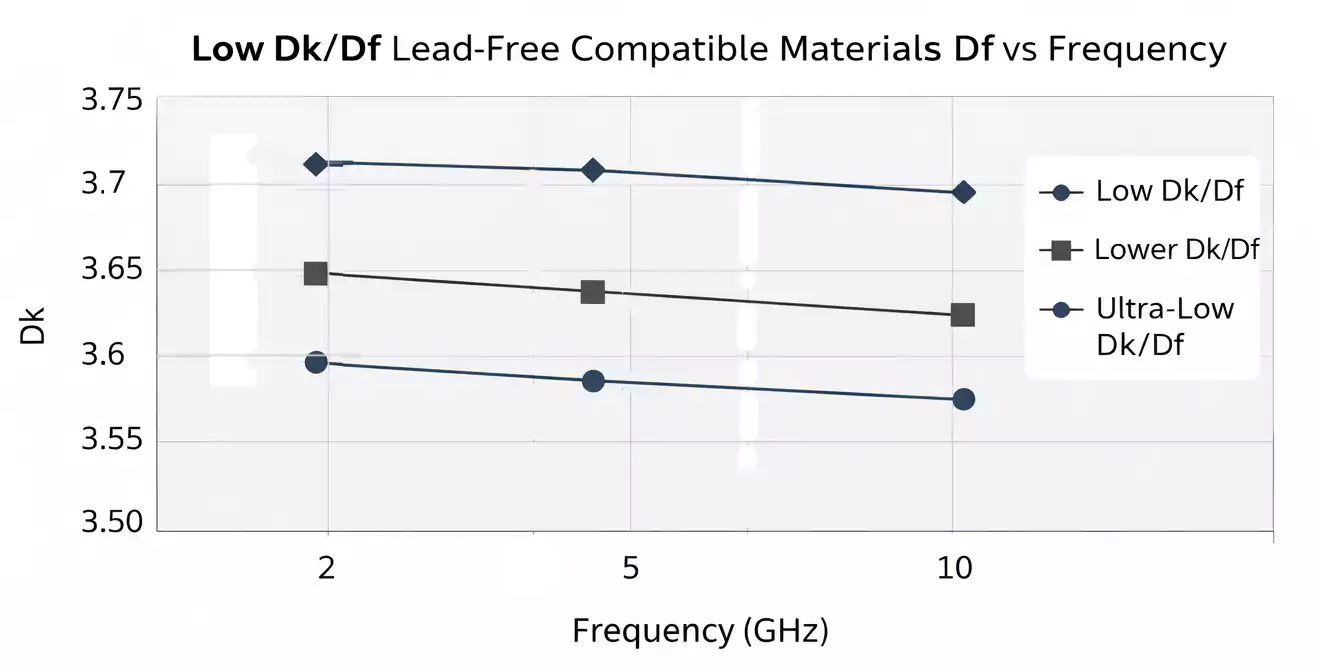
Dk and Df Depend on Frequency
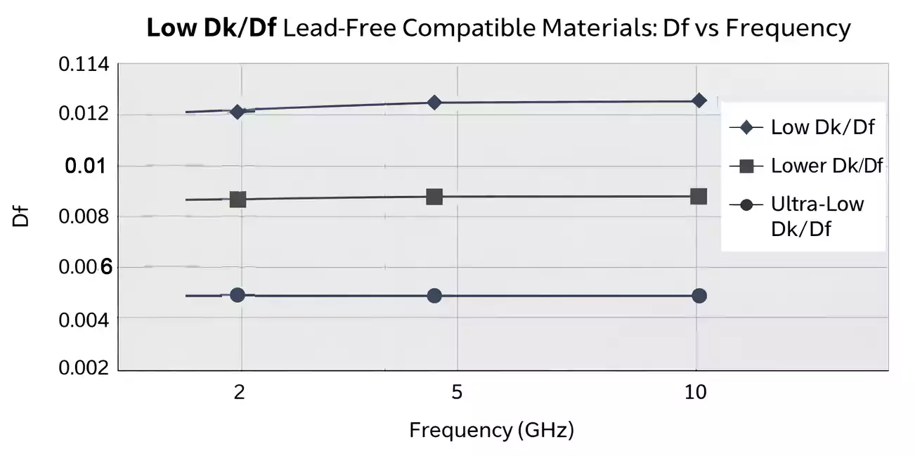
A common misconception is that Dk and Df are fixed constants. In reality, both values change with frequency and test conditions.
As frequency increases:
- Df rises due to higher polarization loss.
- Dk slightly decreases because molecular dipoles can’t follow rapid electric field changes.
For instance, a laminate rated Dk = 3.50 at 1 GHz may show Dk = 3.25 at 10 GHz, with Df nearly doubling.
That’s why engineers should always request frequency-specific Dk/Df data from suppliers or validate it via S-parameter testing or microstrip methods.
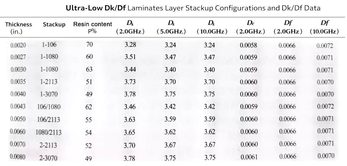
Resin Content Directly Affects Dielectric Performance
Even within the same laminate family, resin content dramatically affects dielectric performance.
Different prepreg/core ratios lead to variations in both Dk and Df:
- Higher resin content:
- Lowers Dk (more resin and air)
- Reduces Df (less glass-fiber loss)
- Higher glass content:
- Increases Dk
- Creates anisotropy and glass weave effects
This is why PCB material selection must consider the actual stackup configuration, not just the datasheet value.
Always confirm with your material supplier or PCB manufacturer that the resin content and layer structure match your target signal frequency.
Electrical + Thermal Co-Optimization Is Key.
Modern PCB material selection isn’t only about Dk and Df numbers — it’s about achieving balanced electrical and thermal performance.
Key takeaways:
- Low Dk/Df = lower signal loss, but not all laminates handle lead-free reflow.
- High Tg, Td, and stable CTE are equally vital for long-term reliability.
- Resin content and frequency directly influence Dk/Df behavior.
- Collaborate early with your PCB supplier to verify both electrical and mechanical specs.
At FastTurn PCB, we help customers co-optimize stackup, impedance, and thermal reliability for high-speed, lead-free production.
FAQ: Low Dk/Df and Lead-Free Compatibility
Which matters more, Dk or Df?
Both are important. Dk impacts impedance and timing, while Df drives signal loss. At multi-GHz speeds, Df usually limits performance first.
Does lead-free reflow change dielectric performance?
Yes. High reflow temperatures can cause delamination or dielectric drift if Tg/Td are too low. Always choose lead-free compatible PCB materials.
Why does the same material show different Dk/Df values?
Because resin content, glass weave style, and core thickness vary across stackups, the effective dielectric constants change.
What’s the best validation before production?
Run a pilot build including thermal cycling and impedance testing. This ensures lead-free reliability and stable dielectric properties under real reflow conditions.
Final Thoughts
As data rates move into the tens of gigabits per second, PCB materials are becoming the new performance bottleneck.
Choosing Low Dk Df PCB Materials is the foundation for building reliable, high-speed hardware — from 5G base stations to automotive radar and data center interconnects.
At FastTurn PCB, we specialize in low-loss PCB fabrication, dielectric validation, and lead-free stackup design to help you deliver faster, cleaner signals with confidence.
