In the world of high-speed digital communication, Signal Integrity (SI) is the ultimate test of system reliability. Among all the factors that affect SI, the electrical properties of the PCB substrate are often underestimated.
Whether it’s 10 Gbps Ethernet, PCIe Gen 5/6, or DDR5 memory, signal quality is no longer about “does it connect?” — it’s about whether the waveform still looks like it should. This article explains how a substrate’s dielectric constant (Dk) and dissipation factor (Df) directly determine the performance limits of a high-speed PCB, using rise time, bandwidth, and eye-diagram analysis as the lens.
Rise Time, Bandwidth, and What They Mean
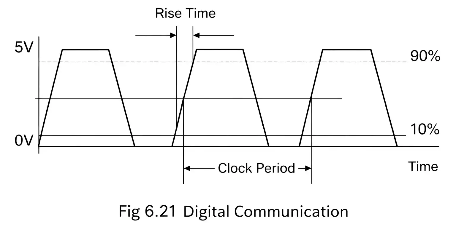
In a digital transmission system, logic “1” represents a high voltage, while “0” represents a low voltage. A high-speed digital signal isn’t a perfect square wave — each voltage transition is made up of a sum of many sine waves. The shorter the rise time, the more high-frequency components the signal contains — and the wider its bandwidth must be.
A simple and widely used relationship captures this:
Bandwidth (GHz) ≈ 0.35 / Rise Time (ns)
For example, a 35 ps rise time corresponds to about 10 GHz of required bandwidth.
In other words:
Shorter rise time → faster signal → more high-frequency energy.
Any factor that limits those high frequencies — such as dielectric loss — will slow the edge and distort the waveform.
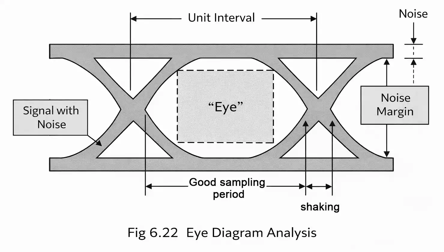
The Eye Diagram: The Health Check of High-Speed Links
An eye diagram is one of the most common tools for evaluating high-speed link quality. By overlaying many waveform segments, the pattern forms an “eye,” revealing the combined effects of noise, jitter, and distortion.
Eye Height
Noise margin — how much noise the system can tolerate
✅ Yes
Eye Width
Jitter margin — how much timing uncertainty can be tolerated
✅ Yes
Edge Thickness
Represents distortion and receiver noise
❌ Thinner = Better
Top/Bottom Flatness
Voltage stability of logic levels
✅ Flatter = Better
A wide-open eye means clean, reliable signal transmission. A closed eye indicates severe degradation — high jitter, high noise, and likely bit errors.
How PCB Materials Impact Signal Integrity
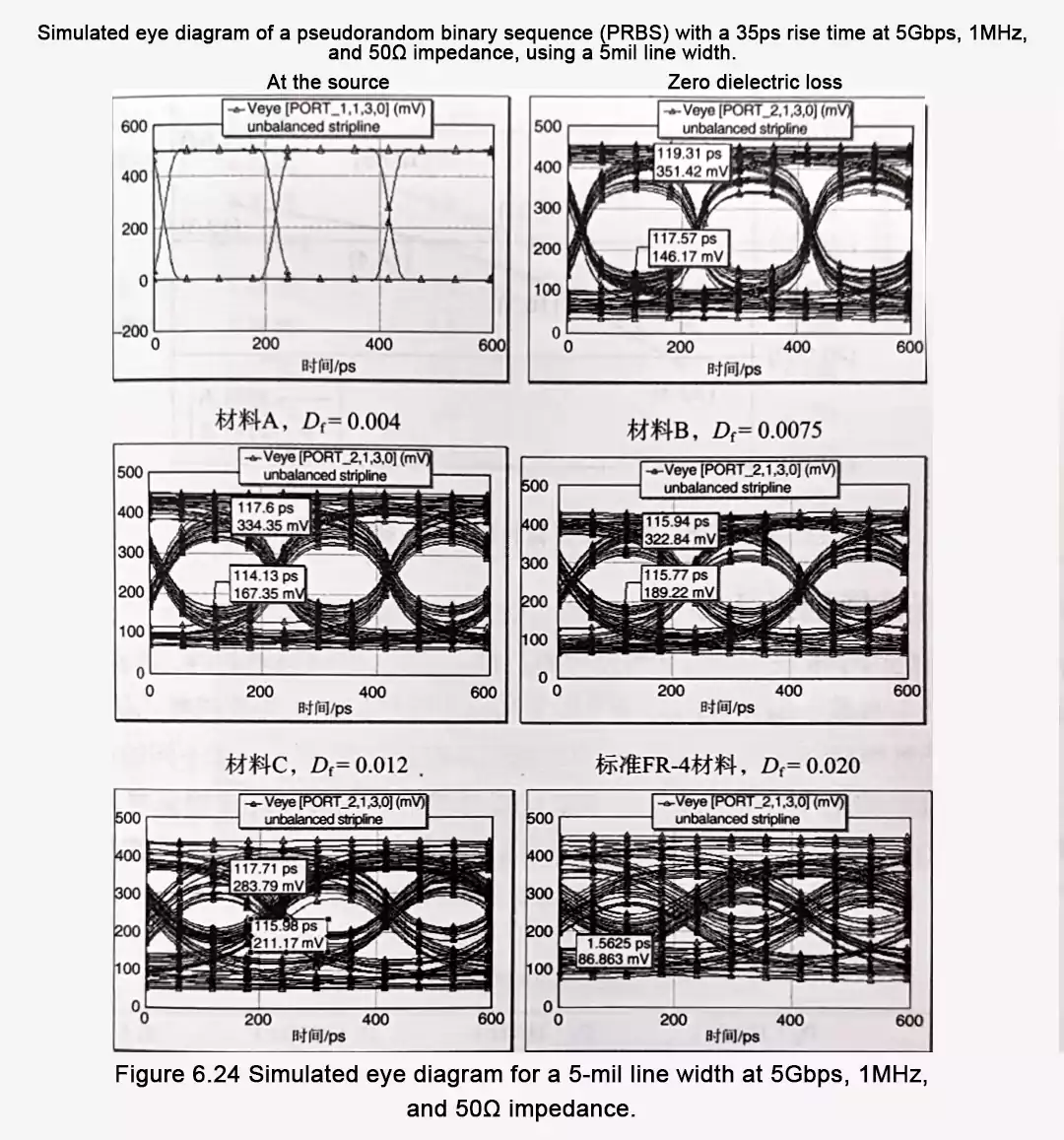
Let’s visualize a 10 Gbps signal (as in the original reference Figure 6.23):
Top waveform: the ideal source signal, cleanly transitioning from 0 to 1.
Lower left (standard FR-4): amplitude reduced, edges rounded, and high-frequency content lost.
Lower right (low Dk / low Df material): waveform closely matches the source with minimal loss.
Here, “D” refers to the substrate’s dielectric properties — primarily Dk (dielectric constant) and Df (dissipation factor or tan δ). In practical high-speed design, Df dominates signal attenuation, while Dk controls propagation speed and impedance.
As Figure 6.24 further shows:
When D (or Df) is high, the eye diagram nearly closes — an unacceptable condition.
When D is reduced, the eye opens, restoring signal clarity and reducing bit errors.
Reducing the material’s loss tangent (Df) is fundamental to preserving signal integrity at high speeds.
Balancing Loss, Line Width, and the Skin Effect
Signal loss on a PCB comes from two main sources:
Dielectric Loss — energy absorbed by the substrate material, proportional to the loss tangent (tan δ).
Conductor Loss — energy dissipated as current crowds to the copper surface at high frequencies (the skin effect).
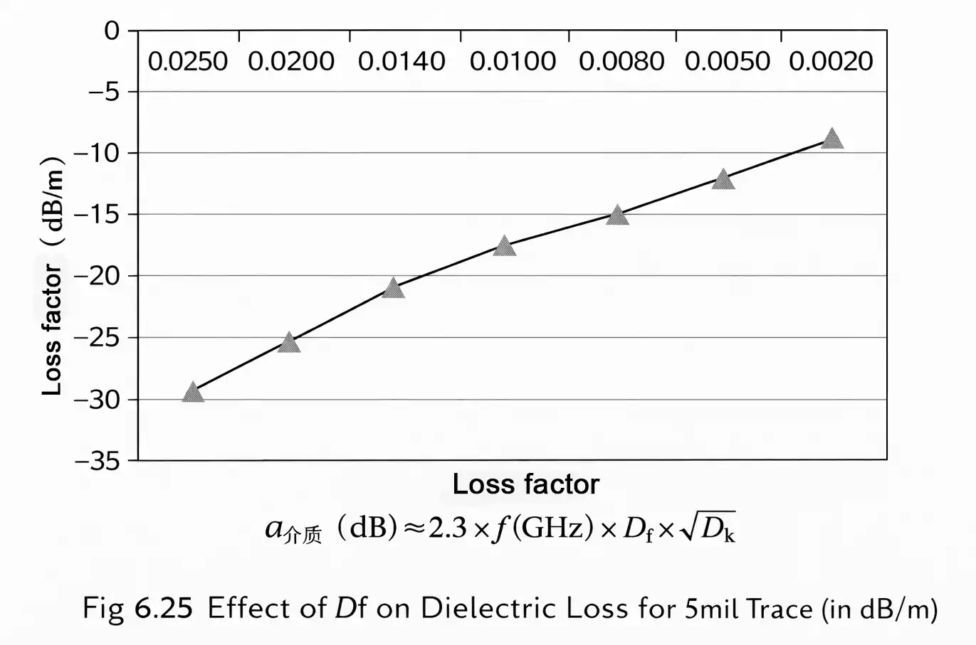
In simulations (referencing Figure 6.25), a 5 mil trace width was used as the baseline to evaluate loss. The results showed:
Wider traces → less skin-effect loss → lower total attenuation.
Increasing line width can offset some dielectric loss, but it reduces routing density.
This trade-off is particularly critical in dense, multilayer, high-speed designs.
Design Freedom with Low-Loss Materials
When using different low Dk / Df materials, the relationship between line width and loss changes dramatically (as in Figure 6.26):
To maintain total loss < 15 dB/m:
Material A (standard low-loss) requires a line width of about 8 mil.
Material B (ultra-low Df) needs only 5 mil.
This enables:
Higher routing density without extra loss.
Finer trace geometries without compromising signal quality.
Better scalability for HDI (High-Density Interconnect) and backplane designs.
The “Material Ceiling” in High-Speed Systems
At 10 Gbps and beyond, the PCB substrate is no longer a passive carrier — it becomes a core part of the signal path itself.
Ultra-low-loss materials (Df < 0.002) with tight impedance control
Conclusion: The Substrate Sets the Limit
In modern high-speed PCB design, the substrate is no longer “just fiberglass” — it’s an active electrical component.
Lower Dk → faster signal propagation and better timing margins.
Lower Df → less loss and a wider, cleaner eye diagram.
Stable dielectric behavior → predictable designs and repeatable production performance.
As data rates push into the multi-Gbps and even Tbps range, Material choice has shifted from a cost decision to a system-performance decision. Choosing the right low-loss substrate helps keep your system’s “eye” open.