


Printed circuit boards (PCBs) are the backbone of all electronic products, from wearables to industrial control systems.
One of the most basic but important design choices is the PCB board thickness.
The board’s thickness affects mechanical strength, impedance, heat dissipation, and even the assembly's fit within the enclosure.
While 1.6 mm (about 0.062 inch) is considered the most common PCB thickness, it is not the only option.
Choosing the right thickness early in your design helps you avoid expensive redesigns later.
This guide explains the PCB Standard Thicknesses, why 1.6 mm became the “industry default,” and how to choose between 0.8, 1.0, 1.2, 1.6, and 2.0 mm options depending on your product.
Why PCB Thickness Matters
PCB thickness determines far more than just how strong a board feels.
It influences:
- Electrical performance: signal impedance and dielectric spacing.
- Mechanical rigidity: the ability to withstand handling or vibration.
- Thermal behavior: how the board spreads and releases heat.
- Connector and enclosure fit: these are designed for specific board thicknesses.
- Manufacturing cost and yield: standard thicknesses simplify stacking and materials, lowering costs.
The term “finished thickness” refers to the total thickness of the board after all processes—including copper plating, solder mask, silkscreen, and surface finish. That number is what matters for mechanical and assembly fit.
What “PCB Standard Thicknesses” Really Means
There is no single global law defining PCB Standard Thicknesses, but the electronics industry has converged on several practical standards.
The most universal value is 1.57 mm (0.062 inch), often rounded to 1.6 mm.
This value comes from the early days of fiberglass-epoxy laminates (FR-4).
Manufacturers standardized their lamination presses, copper foils, and drill tooling around this thickness.
Most edge connectors and card guides are still built for 1.57–1.6 mm boards today.
However, PCB fabrication houses offer a range of standard materials and prepregs, so other thicknesses are also common.
Typical manufacturing tolerance is around ±10 % for boards thicker than 0.8 mm.
For very thin boards, absolute tolerances such as ±0.075 mm (±0.003 inch) may apply.
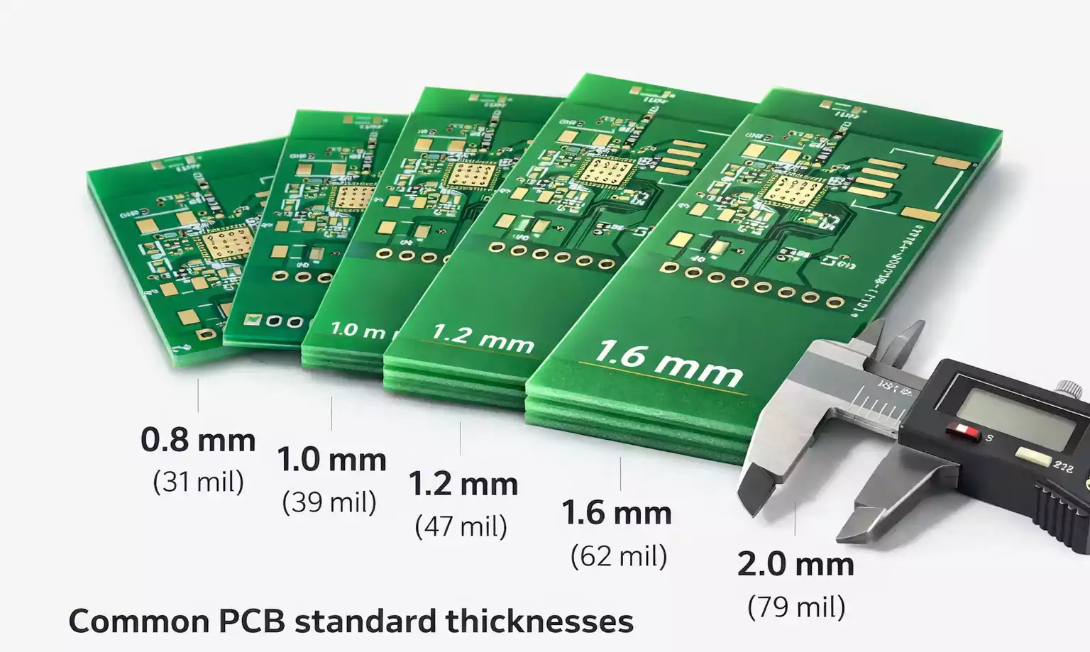
Common Finished Thickness Options
Most PCB manufacturers support the following standard options (metric and inch equivalents):
| 0.4 mm | 16 mil | ultra-thin, flex/rigid-flex applications |
| 0.6 mm | 24 mil | thin modules, space-critical designs |
| 0.8 mm | 31 mil | wearable and card devices |
| 1.0 mm | 39 mil | thin consumer products |
| 1.2 mm | 47 mil | balanced consumer boards |
| 1.6 mm (1.57 mm) | 62 mil | industry standard |
| 2.0 mm | 79 mil | heavy-duty and high-layer boards |
Other imperial standards, such as 93 mil (2.36 mm) and 125 mil (3.18 mm), are also used for thicker multilayer or backplane boards.
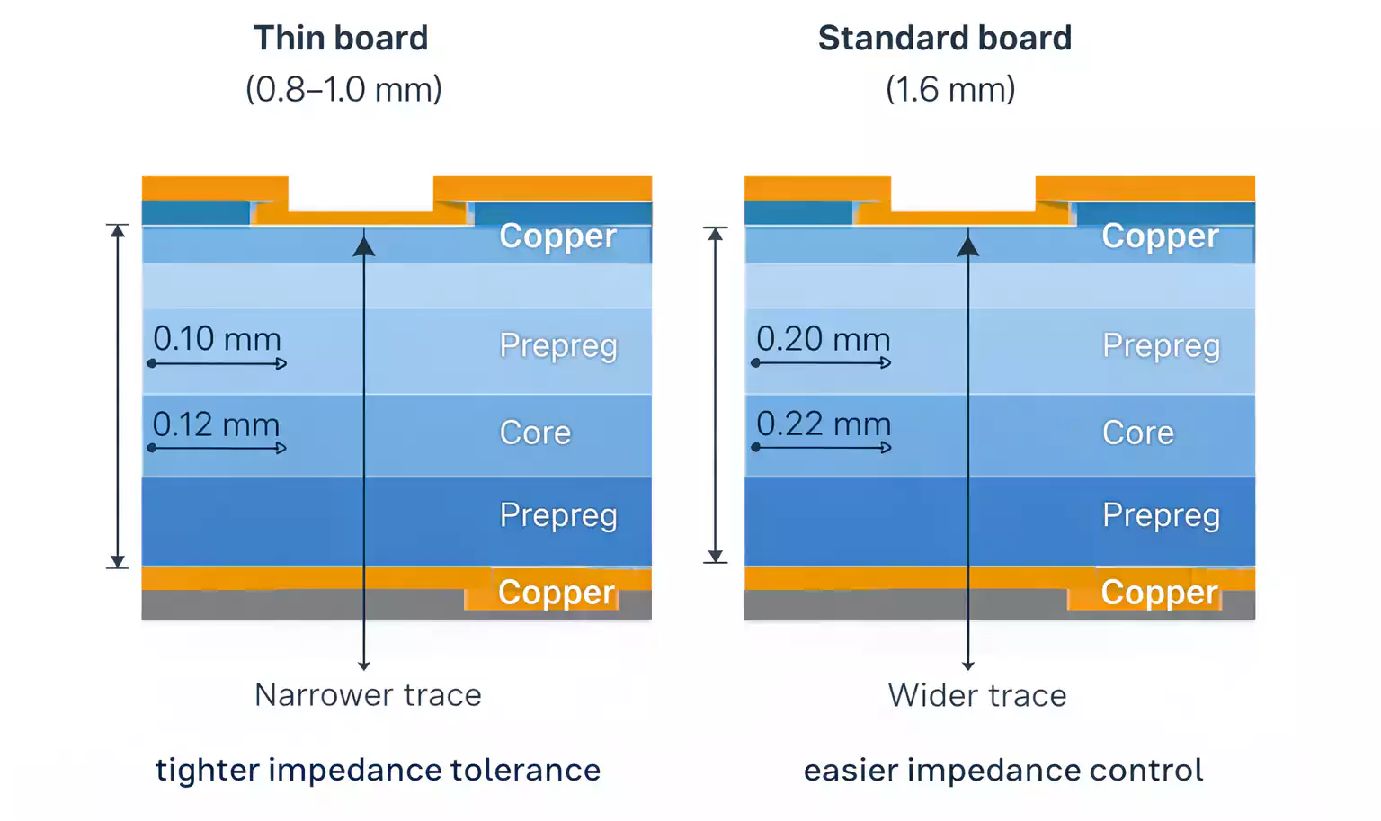
How Thickness Affects Electrical Design
Board thickness directly interacts with layer stack-up and impedance control.
- In a thin PCB, the dielectric between copper layers is smaller.
To achieve the same target impedance (like 50 Ω microstrip or 100 Ω differential), you must use narrower traces, which are harder to manufacture and more sensitive to variation. - A thicker board allows greater spacing and wider traces, improving yield and simplifying impedance control.
Copper thickness also contributes to total thickness.
For heavy-copper boards (e.g., 2 oz/ft² or more), the plating and base copper can add 0.1 mm or more per side.
When designing for controlled impedance, always define the core and prepreg dielectric thicknesses in your stack-up, not just the final board thickness.
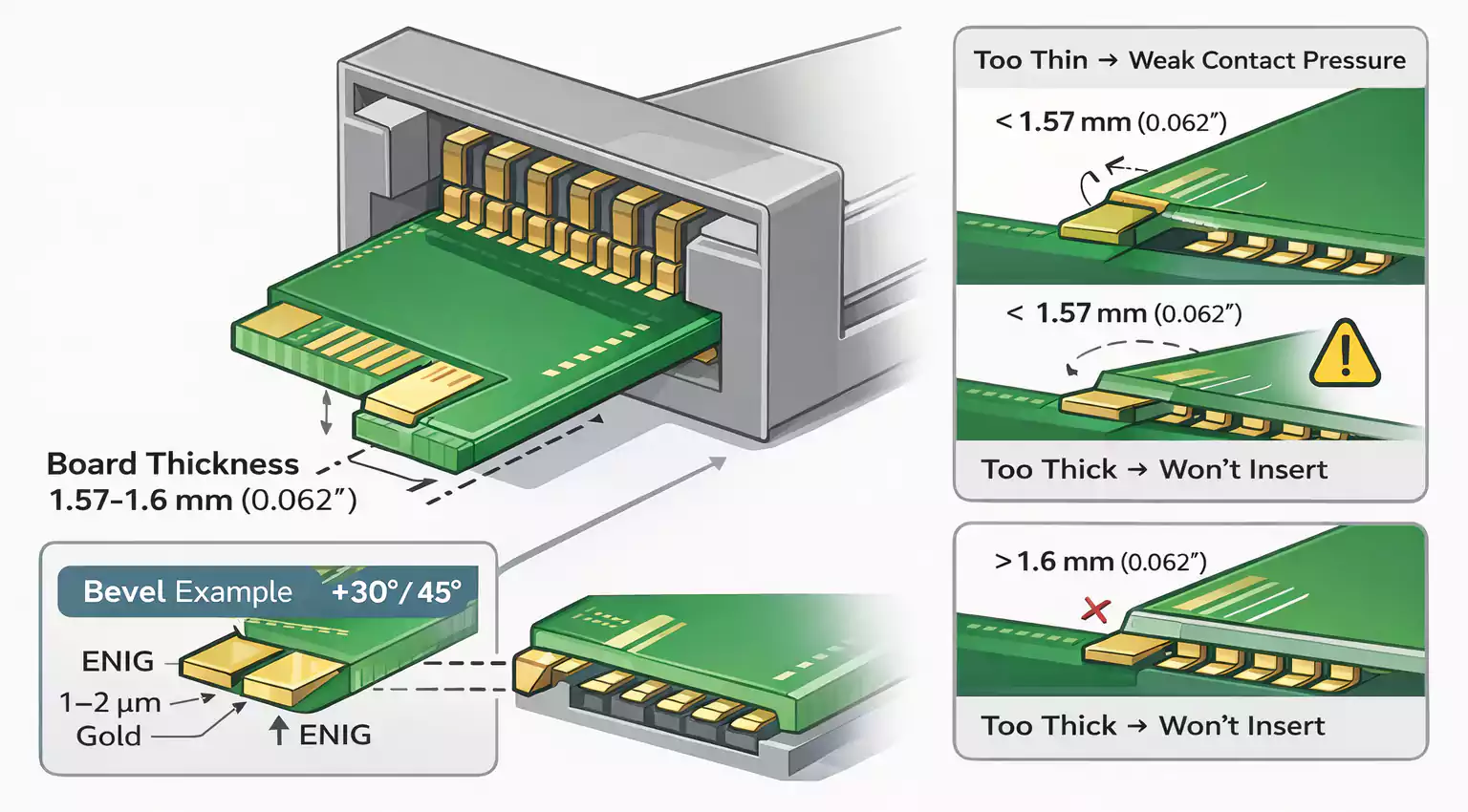
Mechanical and Assembly Fit
Mechanical compatibility is one of the top reasons 1.6 mm became dominant.
- Edge-card connectors and PCI/PCIe slots are designed for 1.57 mm boards.
If your board is thinner, the connector contacts may loosen or misalign; if thicker, it may not insert. - Screw posts, standoffs, and snap-fits in plastic enclosures are expected to work with certain board heights.
Changing thickness could shift component alignment or screw engagement depth. - Handling and warpage: Thinner boards bend easily during pick-and-place or reflow.
For production, manufacturers use panel rails and stiffeners to keep thin PCBs flat.
As a general rule, if your design has no strict space limitation, stick with 1.6 mm for mechanical stability and easy assembly.
Thermal and Reliability Considerations
Board thickness also affects thermal behavior and reliability.
- Thicker boards spread heat better and resist thermal deformation.
They are preferred for high-power circuits, LED boards, or heavy components. - Thin boards heat up and cool down faster, which can lead to warpage after reflow soldering.
- Uneven copper distribution—such as heavy copper areas next to bare FR-4—can cause thin boards to twist even more.
To reduce this, designers use symmetrical layer stacks and balanced copper fills.
Finished thickness includes the solder mask and surface finish (ENIG, HASL, OSP, etc.).
Each finish adds a few micrometers, which can slightly change the connector fit.
How Material Choice Affects Thickness
Core and prepreg materials determine the final thickness.
Different FR-4 grades or high-speed materials (Rogers, Megtron, Isola) have different dielectric constants and resin contents.
To keep impedance targets consistent, you may need to adjust the number of prepreg sheets or copper foil thickness.
Selecting materials with similar glass transition temperature (TG) and expansion behavior helps maintain flatness across temperature cycles.
When ordering, ask your PCB house for a detailed stack-up drawing showing each layer’s dielectric and copper thickness.
This ensures that the finished board thickness matches both electrical and mechanical requirements.
Frequently Asked Questions
Is 1.6 mm the real industry standard?
Yes. 1.57–1.6 mm has been the de facto standard for decades because connectors, fixtures, and materials all evolved around it.
It offers the best balance of rigidity, manufacturability, and availability.
What is the typical tolerance for PCB thickness?
Most manufacturers apply ±10 % tolerance for boards thicker than 0.8 mm.
For very thin boards (≤0.6 mm), the absolute deviation is usually around ±0.075 mm.
Which PCB Standard Thicknesses should I choose for edge-card connectors?
Always use 1.57–1.6 mm unless the connector datasheet states otherwise.
That range ensures proper contact pressure and insertion force.
Summary: Picking the Right Thickness
To select the right PCB Standard Thicknesses, start with mechanical and assembly constraints, then verify electrical and thermal requirements.
- If you have no strict space limit, go with 1.6 mm — it’s the safest and most cost-effective option.
- For ultra-compact or wearable products, 0.8–1.0 mm works well but requires panel support to prevent warping.
- For industrial or high-power designs, 2.0 mm adds stiffness and heat capacity.
- Always confirm stack-up details and tolerances with your manufacturer before releasing Gerber files.
At FastTurnPCB, our engineering team can help you pick the optimal PCB standard thickness for your design and provide a verified stack-up chart before production.We offer standard options from 0.4 mm to 2.0 mm, with custom builds available on request.
Choosing the right thickness early makes your design easier to fabricate, assemble, and maintain.
