


In today’s electronics industry, printed circuit boards (PCBs) are becoming smaller, faster, and more complex — demanding higher wiring density and more reliable interconnections. To achieve this, High-Density Interconnect (HDI) technology has emerged as a cornerstone in advanced PCB design and manufacturing.
Among the most critical enablers of HDI performance are blind vias, buried vias, and microvia materials, which allow engineers to pack more circuitry into limited space without compromising reliability.
Increasing Wiring Density with Blind and Buried Vias
In conventional multilayer PCBs, through-holes pass through all layers, taking up valuable routing space and reducing design flexibility.
HDI technology overcomes this limitation by introducing blind vias and buried vias:
- Blind vias connect outer layers to specific inner layers and are visible from the board’s exterior but do not pass completely through.
- Buried vias connect only internal layers and are invisible from the outside.
By replacing full through-holes with selective interlayer vias, unused internal layers remain available for additional routing. This technique dramatically increases circuit density — one of the defining features of HDI PCB design.
Microvia: The Foundation of High-Density Interconnect Design
The goal of HDI PCB design is to achieve the highest possible interconnection density per unit area.
A key way to achieve this is by reducing via diameters, leading to microvia — extremely small vias typically less than 100 μm in diameter.
Microvias connect adjacent layers (for example, 1–2 or n–n-1), enabling thinner dielectric layers and shorter signal paths. The result is better signal integrity, lower crosstalk, and improved high-frequency performance — essential for today’s 5G, AI, and high-speed computing applications.
Advanced Techniques for Microvia Formation
Manufacturing blind, buried, and micro vias requires specialized technologies. The most widely used processes include:
1. Laser Drilling
- The most common and reliable method for microvia formation.
- Rapidly ablates resin and can even penetrate parts of the glass fiber weave.
- Produces clean hole walls suitable for precise HDI interconnections.
2. Plasma Etching
- Effective for removing resin but less effective at etching glass fibers.
- This limitation led to the development of new reinforcement materials that can replace traditional glass cloth to improve etching precision.
3. Photo-Via (Photo-Defined Via) Formation
- Uses photochemical reactions in a light-sensitive dielectric layer to directly define microvias.
- Compatible with electroplating and lamination processes for selective interconnects.
Among these, laser drilling remains the industry standard thanks to its speed, precision, and scalability for mass production.
Materials for Blind and Buried Via Construction
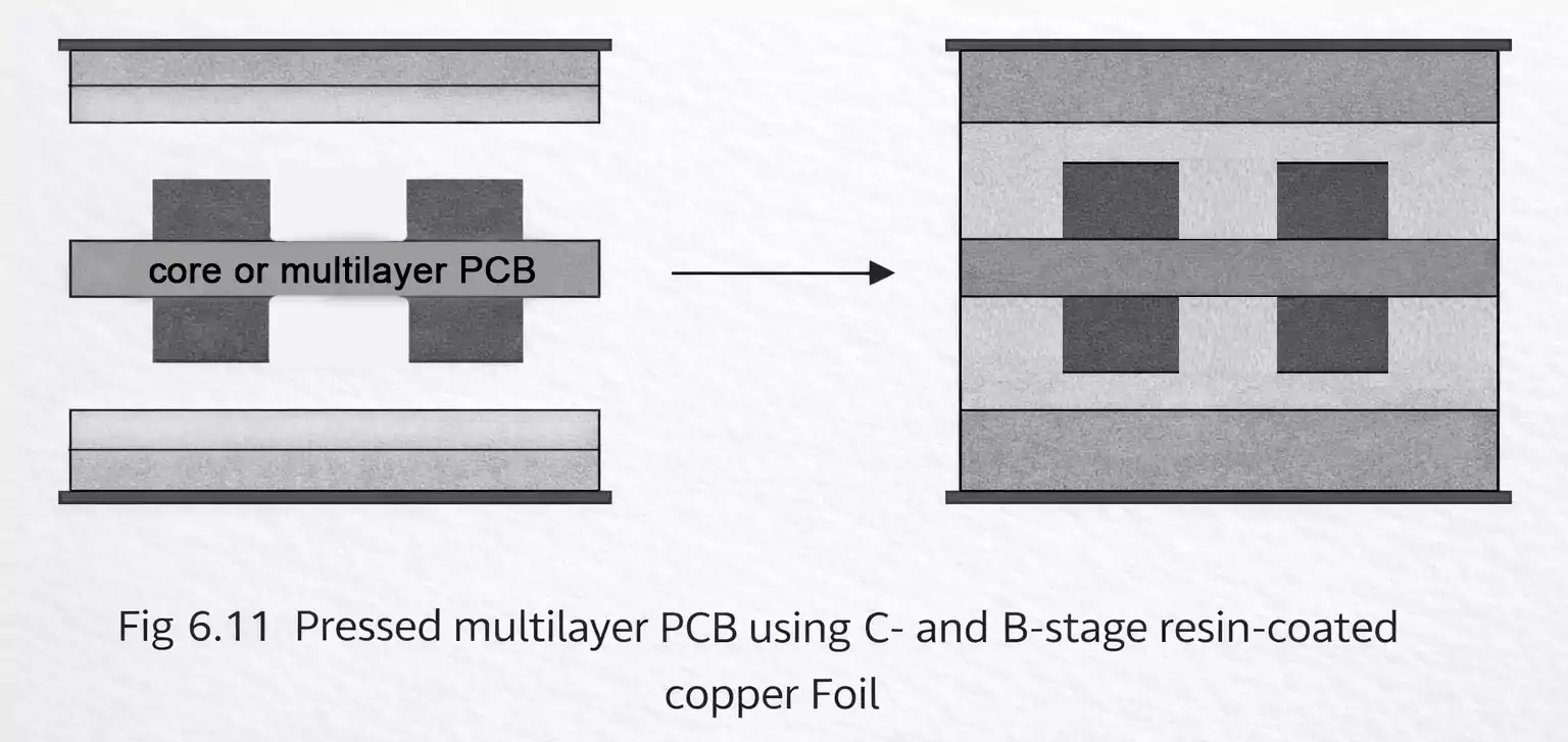
1. Resin-Coated Copper (RCC)
RCC materials are widely used in HDI PCB stack-ups to form the bonding layer between copper foils and dielectric materials. They are particularly suited for laser-drilled blind vias.
Typical applications include:
- Forming interconnections between layer 1–2 or layer n–n-1;
- Using laser drilling or plasma etching to form blind vias;
- Electroplating vias to achieve robust metallization.
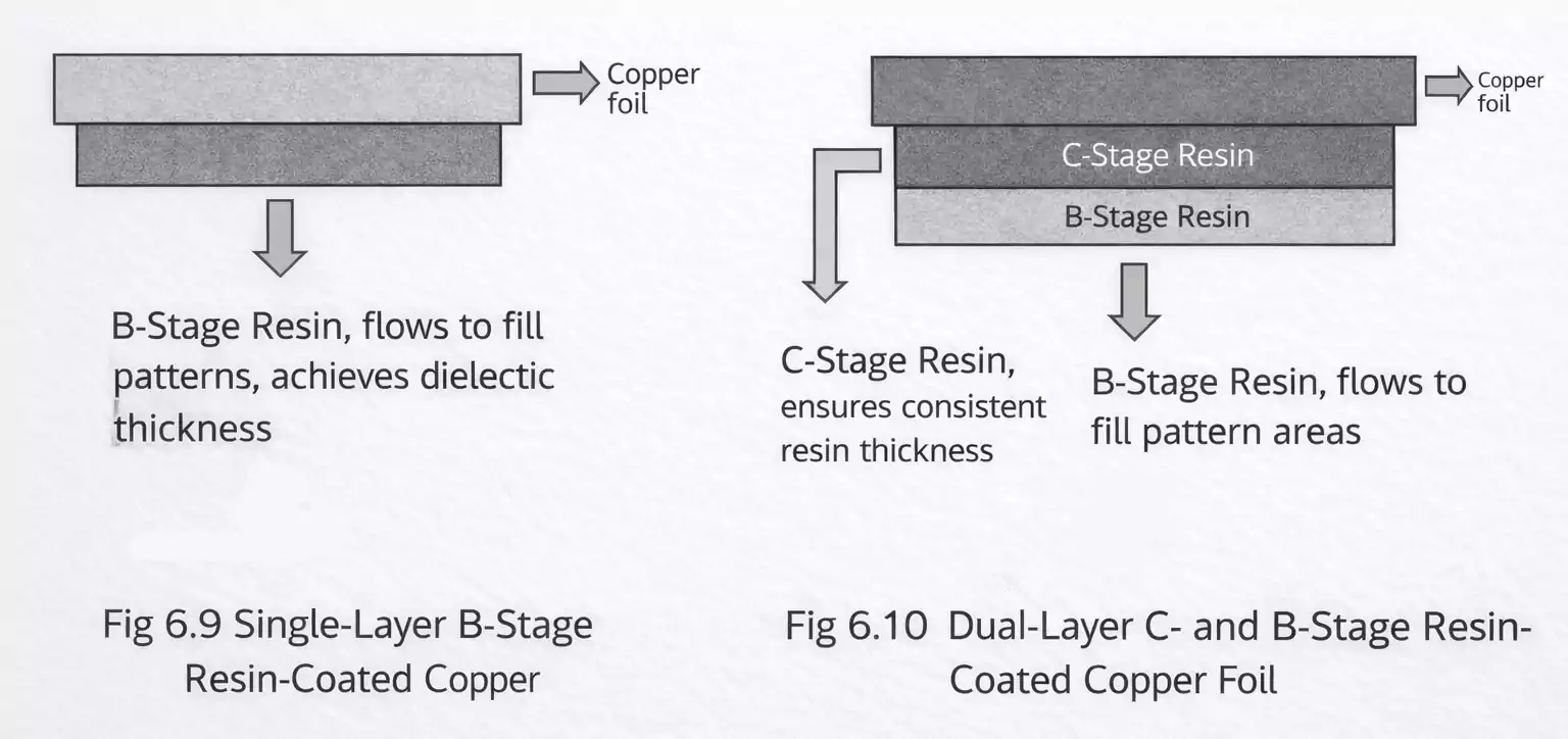
There are two main RCC types based on resin structure:
(1) Single-Layer Resin RCC
- Contains one partially cured (B-stage) resin layer laminated into the multilayer stack.
- Simple and effective for standard HDI processes.
(2) Dual-Layer Resin RCC
- Combines one fully cured resin layer with one partially cured layer.
- The cured layer precisely controls the electrical spacing between the inner and outer layers.
- Ensures minimum dielectric thickness and improved insulation reliability.
- Provides greater consistency in electrical performance across layers.
New Reinforcement Materials for HDI Manufacturing
Because glass fiber reinforcement is difficult to etch or laser-drill, the HDI industry has developed alternative reinforcement materials that enhance manufacturability.
1. Aramid Fiber (Aromatic Polyamide)
- A randomly oriented organic fiber reinforcement that can be removed by laser ablation or plasma etching.
- When impregnated with resin, it forms laminates or prepregs suitable for high-density multilayer PCBs.
- Due to the higher cost, it is primarily used in high-performance or specialty HDI boards.
- Common aramid-based laminates have a 50% resin content and are available in multiple thicknesses to meet layer-spacing requirements.
2. Expanded PTFE (ePTFE)
- A microporous, sponge-like material used for prepregs and HDI bonding layers.
- Offers an ultra-low dielectric constant (Dk) and minimal dissipation factor (Df).
- Ideal for high-frequency and high-speed signal transmission applications.
ePTFE materials help designers achieve both electrical performance and density in advanced multilayer HDI circuits.
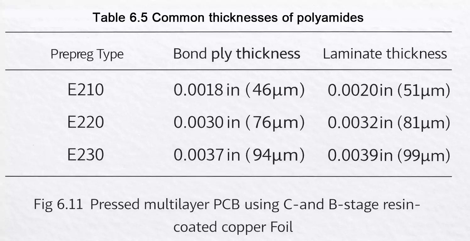
Photo-Definable Dielectrics for Microvia Formation
A third approach for forming microvias involves using photo-definable dielectric materials — permanent photopolymer layers that can be exposed and developed like photoresist.
Key characteristics include:
- Photosensitivity for selective via patterning;
- Catalytic capability for subsequent metallization;
- Strong adhesion to adjacent layers, ensuring long-term reliability under thermal and mechanical stress.
This approach bridges the gap between conventional drilling and advanced photolithography, offering a flexible path toward next-generation fine-line HDI PCBs.
Conclusion
As electronic products continue to shrink while increasing in speed and complexity, High-Density Interconnect (HDI) and microvia material technologies have become essential to modern PCB manufacturing.
By leveraging blind and buried vias, microvia processes, and next-generation reinforcement materials, engineers can achieve:
- Higher wiring density and improved layout flexibility;
- Shorter signal paths and superior high-frequency performance;
- Reduced layer count without sacrificing reliability;
- Enhanced manufacturability for advanced electronic systems.
With ongoing innovations in laser drilling precision, low-Dk materials, and photo-definable dielectric technologies, the design freedom and performance of HDI PCBs will continue to evolve — paving the way for more compact, powerful, and efficient electronic devices.
As a professional PCB manufacturer and quick-turn service provider, FastTurnPCB continues to invest in R&D for HDI and microvia technologies, delivering high-precision, high-reliability circuit board solutions to global customers.
