


Making your own printed circuit boards (PCBs) is one of the most satisfying parts of electronics. Whether you want to learn how circuits are made, build small prototypes, or simply avoid long manufacturing lead times, a PCB kit gives you everything you need to get started.
This guide covers what a PCB kit includes, how to build a board at home, and when to consider using machines or professional fabrication. We’ll compare beginner kits and share practical troubleshooting tips for first-time success.
What Is a PCB Kit (and Who It’s For)
A PCB kit packages the tools and materials you need to make or assemble printed circuit boards at home or in a lab. Most kits fall into two categories:
- Fabrication kits — include copper-clad boards, transfer materials, etching chemicals, and small tools. You use them to create the PCB itself from blank copper laminate.
- Assembly or soldering kits — come with pre-made boards and electronic components for practice or small DIY projects (LED flashers, amplifiers, Arduino accessories, etc.).
Compared with a breadboard kit, which you use only for temporary wiring, a PCB kit lets you produce a durable, permanent board.
The Simplest Way to Make a PCB at Home
You don’t need industrial equipment to produce a working board. Three basic routes are common among beginners:
- Laser print and iron transfer: You print your PCB layout on glossy paper and iron it onto the copper board so the toner pattern sticks.
- Photoresist exposure: Use UV-sensitive boards and a printed film mask for higher precision.
- Hand drawing: For quick one-off circuits, you can draw traces directly with an etch-resist pen.
You can make a functional single- or double-sided PCB this way with minimal tools and a few hours of work.
What’s Inside a Good PCB Kit
The best kits include all essential items for safe and repeatable results. A typical home PCB kit should have:
- Copper-clad board (FR-1 or FR-4)
- Toner transfer sheets or photoresist film
- Etching solution (ferric chloride or ammonium persulfate)
- Plastic tray or tank for etching
- Gloves, goggles, and a protective apron
- Small drill or rotary tool with fine bits
- Cleaning pads or fine sandpaper
- Soldering iron, solder wire, and flux
- Basic multimeter for testing
Safety First: Protection, Ventilation & Waste Handling
Etching chemicals are effective but corrosive. Follow these essential safety rules:
- Wear gloves and goggles. Always protect skin and eyes from splashes.
- Work in a ventilated area. Etching produces mild fumes; use a fan or open a window.
- Avoid metal containers. Use only plastic or glass tanks.
- Label and store solutions. Keep acids or salts away from children and food.
- Never pour waste into the sink. Neutralize spent ferric chloride with baking soda, then dispose of it in accordance with local household hazardous-waste rules.
If your workspace is small or shared, consider switching to a desktop PCB milling or printing machine—it’s cleaner and chemical-free.
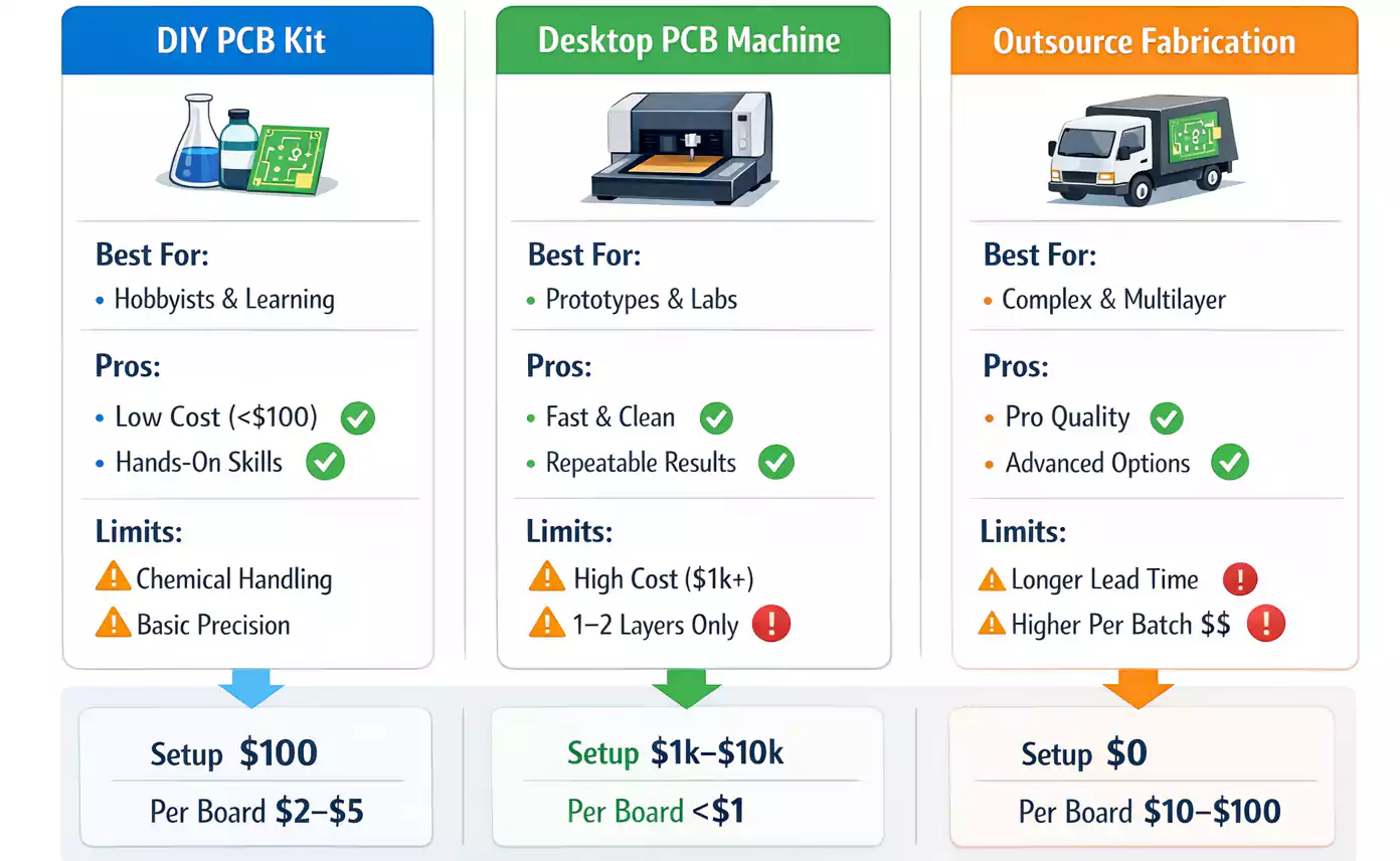
DIY Kit vs. PCB-Making Machine vs. Outsourcing
The right method depends on time, budget, and complexity.
| DIY Kit | Beginners, learning, simple circuits | <$100 | Low cost, hands-on, educational | Manual labor, limited precision |
| Desktop PCB-Making Machine | Labs, makerspaces, small R&D teams | $1,000–$10,000 | Fast turnaround, no chemicals | High upfront cost, size limits |
| Outsourced Fabrication | Professional or multilayer boards | $10–$100 per batch | Industrial accuracy, surface finish | Shipping delay, minimum order |
DIY Kits
Perfect for learning and small analog or microcontroller boards. Expect rougher finishes but plenty of satisfaction.
Desktop PCB-Making Machines
There are two main types:
- Ink-based printers (e.g., Voltera V-One, BotFactory SV2) deposit conductive ink, cure it, and even dispense solder paste. Ideal for quick prototypes but limited to 1–2 layers and coarse pitch.
- CNC milling machines (e.g., LPKF ProtoMat) mechanically remove copper and drill holes. They produce clean, single- or double-sided boards without chemicals, but they require a bit of maintenance and dust control.
Outsourcing
If you need fine traces, multilayer stacks, or plated-through holes, it’s usually cheaper and more reliable to send Gerbers to a PCB fab house.
Types of PCB Kits for Beginners
Here are three kit categories worth knowing:
1. Complete Etching Kits
Contain everything to go from a blank copper sheet to a working board. Great for first-timers who want the full experience. You’ll learn layout alignment, etching control, and cleaning.
2. Soldering Practice Kits
Come with a pre-made PCB and discrete components to practice hand soldering—perfect for students and anyone learning SMT or through-hole techniques.
3. Prototyping Board Sets
Include perfboards, stripboards, and headers. These aren’t real PCB-making kits, but they help quickly test a circuit before investing in etching or manufacturing.
Each type differs in learning curve, result quality, and hidden costs like consumables and cleanup. Beginners often start with an etching kit, then move to a small desktop printer once they understand the process.
Step-by-Step: Your First PCB with a Kit
Let’s combine the theory into a simple workflow you can actually follow.
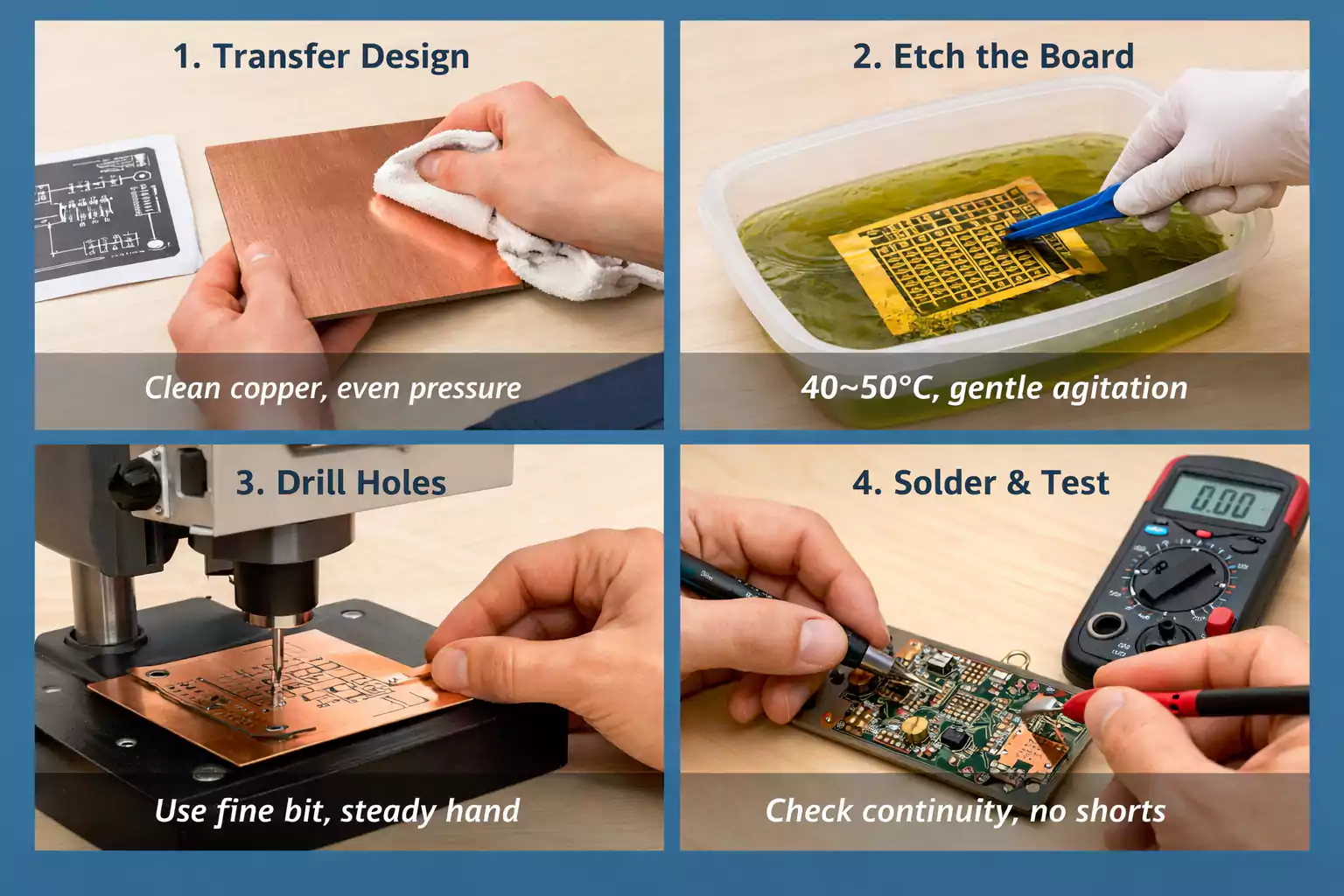
Step 1 — Prepare the design
Export your PCB artwork as a mirrored image. Double-check that footprints, hole diameters, and polarities match your components.
Step 2 — Transfer the layout
Clean the copper surface with fine sandpaper. Print your layout on glossy transfer paper and iron it evenly for 1–2 minutes. Allow to cool, then peel off gently.
Step 3 — Etch
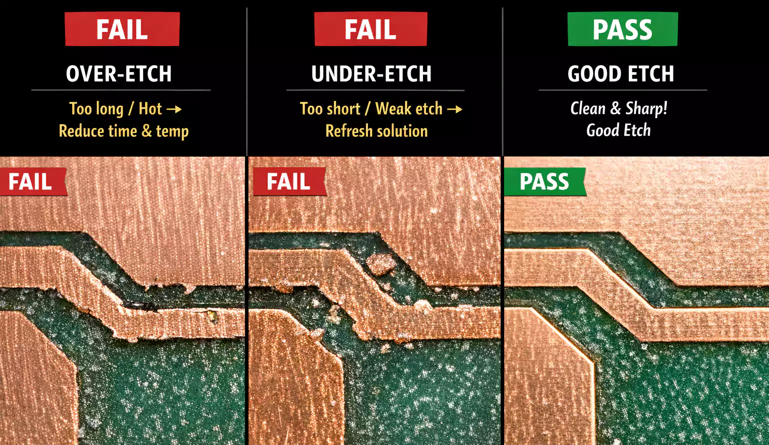
Submerge the board in etching solution at 40–50 °C (105–120 °F). Gently agitate until the unwanted copper disappears—usually 5–10 minutes.
Too long = over-etching (thin traces).
Too short = under-etching (bridged pads).
Step 4 — Drill and finish
Rinse under water, dry, and drill holes using a 0.8–1.0 mm bit. Remove any burrs. For simple double-sided boards, align and tape layers carefully before drilling.
Step 5 — Solder and test
Tin exposed copper if desired, mount your parts, and inspect with a multimeter. Check for shorts and verify all power pins before plugging in power.
With practice, you can finish a small single-sided PCB in about two hours from design to powered test.
Common Mistakes and How to Fix Them
Even experienced makers mess up occasionally. Here are the most frequent problems—and fast remedies.
| Incomplete transfer | Surface not cleaned or temperature too low | Re-clean, re-iron at higher heat, use glossy magazine paper |
| Over-etching / broken lines | Etching too long or too hot | Reduce time/temperature; refresh solution |
| Under-etching / copper bridges | Old solution or insufficient agitation | Replace chemical or stir gently |
| Drill misalignment | Handheld drilling without guide | Use a small vise or mark pilot holes |
| Pads lifting or peeling | Overheated soldering iron | Lower tip temperature, minimize dwell time |
Keep failed boards—they’re excellent learning samples for your next attempt.
FAQs
How fine can DIY PCB kits go?
Typically down to 0.25–0.3 mm trace width with careful alignment. For finer work, use a desktop printer or professional fab.
Is home etching safe?
Yes—if you wear gloves, goggles, and work with ventilation. Never dispose of waste chemicals in the sink.
Can I make PCBs without a drill?
You can use surface-mount components and skip drilling, or use conductive rivets as an alternative.
Can desktop machines make multilayer boards?
Most handle only one or two layers. For complex multilayer builds, outsourcing is more economical.
When should I outsource instead of DIY?
Whenever your design needs impedance control, plated-through holes, or tight, fine-pitch ICs.
Conclusion: Learn, Experiment, and Grow
A PCB kit is more than a box of supplies—it’s a gateway to understanding how modern electronics come to life. You’ll learn the fundamentals of pattern transfer, etching, drilling, and soldering—skills that apply even in professional manufacturing.
Start small: make a single-sided board, test a few patterns, and document your settings. Once you’re comfortable, you can upgrade to a desktop PCB-making machine or send your designs to a fab house with confidence.
