


When your surface-mount assembly line runs at thousands of placements per hour, precision matters. Even the most advanced pick-and-place machine needs a reference to know exactly where the PCB sits.
Fiducial marks—tiny copper dots on the PCB—help machines align components precisely, preventing costly misplacements and rework.
This guide explains what fiducial PCB marks are, why they matter, when to use global vs. local fiducials, and how to size, position, and maintain them for perfect assembly results.
We’ll also explore how fiducials connect to PCB etching, solder mask openings, and board testing to improve yield and reliability.
What Is a Fiducial on a PCB and Why It Matters
A fiducial mark is a small, bare-copper circle (sometimes square or diamond-shaped) placed on the PCB surface to serve as a visual reference for automated optical systems.
Pick-and-place machines, solder paste printers, and AOI systems use cameras to locate these fiducials, establishing the PCB’s X, Y, and rotational orientation (θ) before placing components.
In essence, fiducials allow the machine to “see” the board. Without them, even a 0.1 mm offset can result in misaligned fine-pitch components—especially with BGAs, QFNs, and QFPs.
Although modern machine calibration systems have advanced, fiducials remain essential for compensating for board stretch, rotation, or shrinkage caused by temperature and lamination.
They are among the simplest and cheapest design elements that improve assembly accuracy.
Global vs. Local Fiducials
Not all fiducials serve the same purpose. Designers typically use two types:
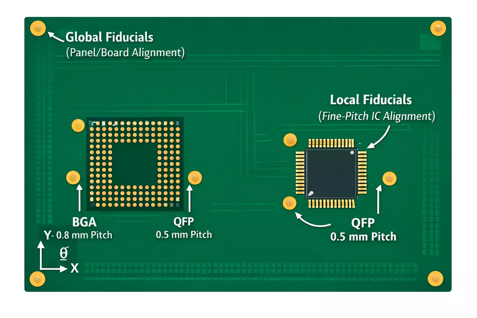
Global Fiducials
- Define the entire PCB or panel orientation.
- Usually placed near three corners of the board, forming a triangle.
- Used by printers and pick-and-place machines to align the entire PCB or panel.
- Often located on the panel rails (if using a multi-up array).
Local Fiducials
- Placed close to individual fine-pitch components, such as BGA or QFP packages.
- Help the machine accurately align those specific parts relative to their pads.
- Critical for components with lead pitch below 0.5 mm or pad spacing under 0.25 mm.
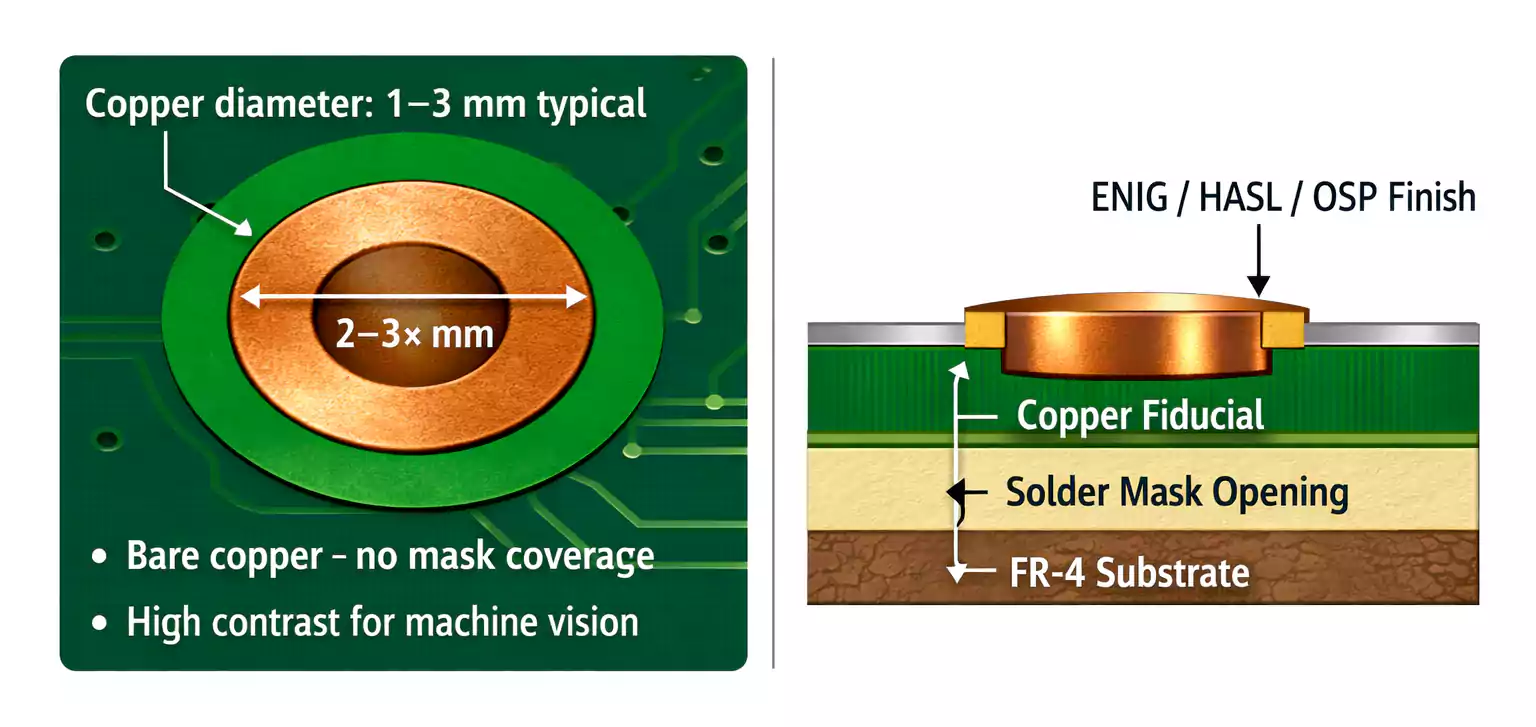
Fiducial Shape, Size, and Solder Mask Opening
Fiducials may seem simple, but their geometry affects the accuracy of machine vision.
- Shape:
A solid circular pad is industry standard because it’s symmetrical and easy for cameras to detect.
Square or diamond shapes may be used if circular ones are impractical, but consistency matters—use the same style across the board. - Copper Diameter:
Common fiducial size ranges from 1.0 to 3.0 mm (0.040"–0.120").
Most manufacturers recommend 1.5 mm (≈0.060") copper pads for visibility. - Solder Mask Clearance:
The fiducial should be completely exposed bare copper—no solder mask coverage. The solder mask opening should be 2× to 3× the copper pad diameter (for example, a 1 mm pad with a 2–3 mm opening) to create a clear contrast between the copper and the surrounding mask. - Surface Finish:
ENIG, HASL, or OSP finishes are all acceptable, but the area must remain clean and reflective for camera detection.
Uniformity is key—use the same diameter and opening size for all fiducials on a single board.
Placement Rules and Best Practices
Place fiducials for clear visibility and precise orientation reading.
Number and Pattern
- Use three fiducials arranged in a non-collinear triangle for the best rotational and scaling correction.
- Two fiducials are the minimum required for orientation, but three provide redundancy and allow correction for board warpage.
Position
- Place fiducials near opposite corners of the board (typically top-left, bottom-right, and bottom-left).
- Maintain a minimum clearance of 3.5–5 mm from the board edge to avoid clamp shadows.
- Keep fiducials at least 6 mm away from nearby copper pours, silkscreen text, or vias.
Top and Bottom Sides
If both sides of your PCB have SMT components, include fiducials on each side.
Ensure that each side’s marks are properly registered in the design data and not mirrored incorrectly.
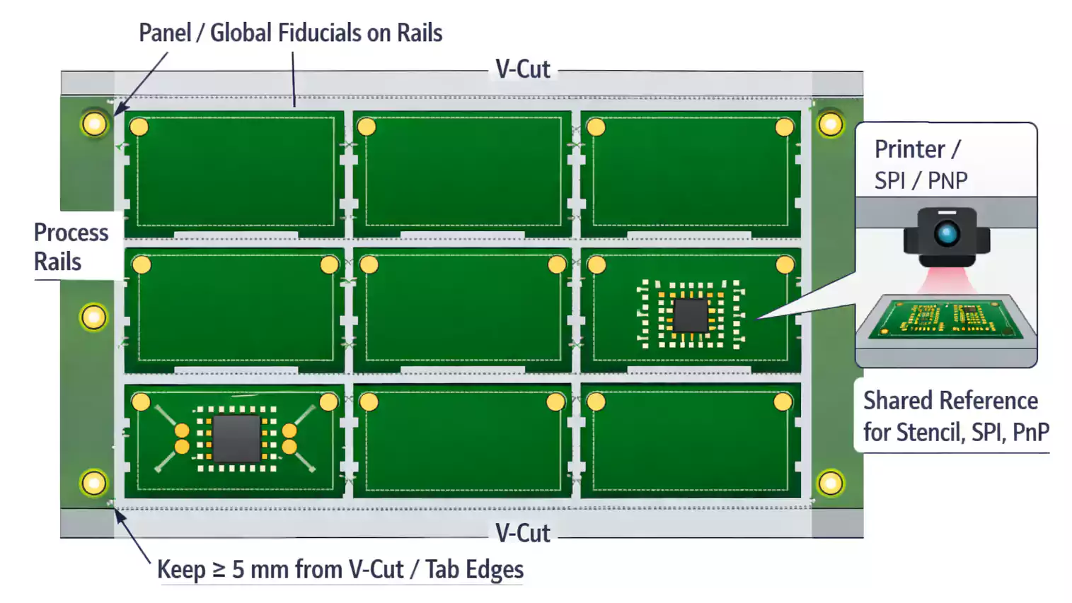
Fiducials on Panel Rails and Multi-Up Arrays
For production efficiency, multiple boards are often fabricated into a single large panel (array).
Fiducials play an even greater role here:
- Place three global fiducials on the panel frame or rails, outside individual PCBs.
These marks define the panel’s coordinate system for stencil printing and pick-and-place alignment. - Each individual board can also have its own global or local fiducials for secondary reference.
- Maintain at least 5 mm clearance between fiducials and V-cut or tab-routing edges to prevent damage or misreads.
Standardized panel fiducials speed up loading and alignment, improving throughput and setup time.
Connection to Other PCB Manufacturing Stages
Fiducial marks don’t exist in isolation. They interact with nearly every process—from PCB etching to testing.
1. During PCB Etching
When copper traces and pads are etched, the fiducial copper disk must remain clean and flat.
Etching residue or over-etching can dull the edges, making the mark harder to detect.
Ensure no silkscreen or solder mask ink bleeds over the copper area.
Surface treatment also matters: ENIG and OSP provide smoother contrast for camera vision, while rough HASL finishes may create reflection issues if uneven.
2. During Solder Paste Printing
Stencil alignment systems use fiducials on panel rails as primary references.
If they’re missing or mis-sized, you’ll see paste misalignment and insufficient coverage on fine-pitch pads.
3. During Pick-and-Place
The machine camera reads fiducials first, then calculates board coordinates.
Global marks set the baseline; local marks fine-tune component placement.
Even a single smudge or oxidation spot can trigger “fiducial not found” errors.
4. During Reflow and Inspection
After soldering, fiducials assist AOI (Automated Optical Inspection) and SPI (Solder Paste Inspection) in frame alignment.
They also provide a consistent reference point for repeatable inspection between production batches.
5. During PCB Board Testing
For In-Circuit Test (ICT) or Flying Probe, fiducials can help align test fixtures and ensure accurate probe contact.
In functional test setups, they allow repeatable camera or mechanical positioning when inspecting multiple boards in a fixture.
Component-Specific Fiducial Recommendations
BGA and Fine-Pitch Packages
- Always place two local fiducials diagonally near the component’s opposite corners.
- Maintain at least 5 mm clearance from pads and traces.
- Use the same size and opening ratio as global marks for consistency.
Large PCBs or Long Boards
- Consider adding additional global fiducials in the center area to account for potential bow or twist.
- Long boards (like LED strips or backplanes) benefit from marks every 100–150 mm for camera recalibration.
Low-Density Designs
- If your board uses only 1206, SOIC, or larger components, and you have a rigid, well-defined panel, global marks may suffice.
Still, retaining fiducials improves flexibility when switching between different assembly lines.
Common Fiducial PCB Mistakes to Avoid
Here are the most common—and easiest to prevent—issues:
- Covered by Solder Mask
– Always leave the fiducial bare; any ink reduces contrast. - Too Small or Too Large
– Stay within the 1–3 mm range; extremes confuse cameras. - Too Close to Edge or V-Cut
– Keep at least 5 mm away from stress or breakout zones. - Silkscreen Overlaps
– Don’t print polarity marks or text over fiducials. - Inconsistent Sizes or Shapes
– Uniform fiducials simplify calibration. - Only One Fiducial on Board
– Two are minimum, three are best. - Missing on the Second Side
– If both sides have components, both sides need fiducials.
A quick design-rule check before generating Gerber files can catch nearly all of these.
Implementing Fiducials in Your EDA Tool
Adding fiducials is simple in most CAD tools like Altium Designer, KiCad, or Eagle:
- Create a copper pad (non-plated) on the top or bottom layer.
- Disable the solder mask for that pad to expose the metal.
- Define diameter (e.g., 1.5 mm) and clearance (e.g., 3 mm).
- In Altium, use the “Fiducial” component from the PCB library.
- Include fiducials in both Gerber/ODB++ and Pick-and-Place outputs to ensure your assembler sees them.
- For double-sided assemblies, label top and bottom marks separately in your fabrication notes.
It’s a small addition that pays off massively in assembly yield and inspection accuracy.
Frequently Asked Questions
Q: How many fiducials are required?
A: Use at least two; three are recommended for full orientation and warpage correction.
Q: How big should fiducials be?
A: Typical copper size is 1–3 mm (1.5 mm preferred), with a 2–3× solder mask opening.
Q: Can I place fiducials under components?
A: Not advised. They must remain visible during all assembly stages.
conclusion
In short, fiducial marks are the unsung heroes of PCB manufacturing—tiny details that enable high-precision manufacturing at scale.
Design them right, and your boards will pass smoothly through every step from stencil printing to final test.
