

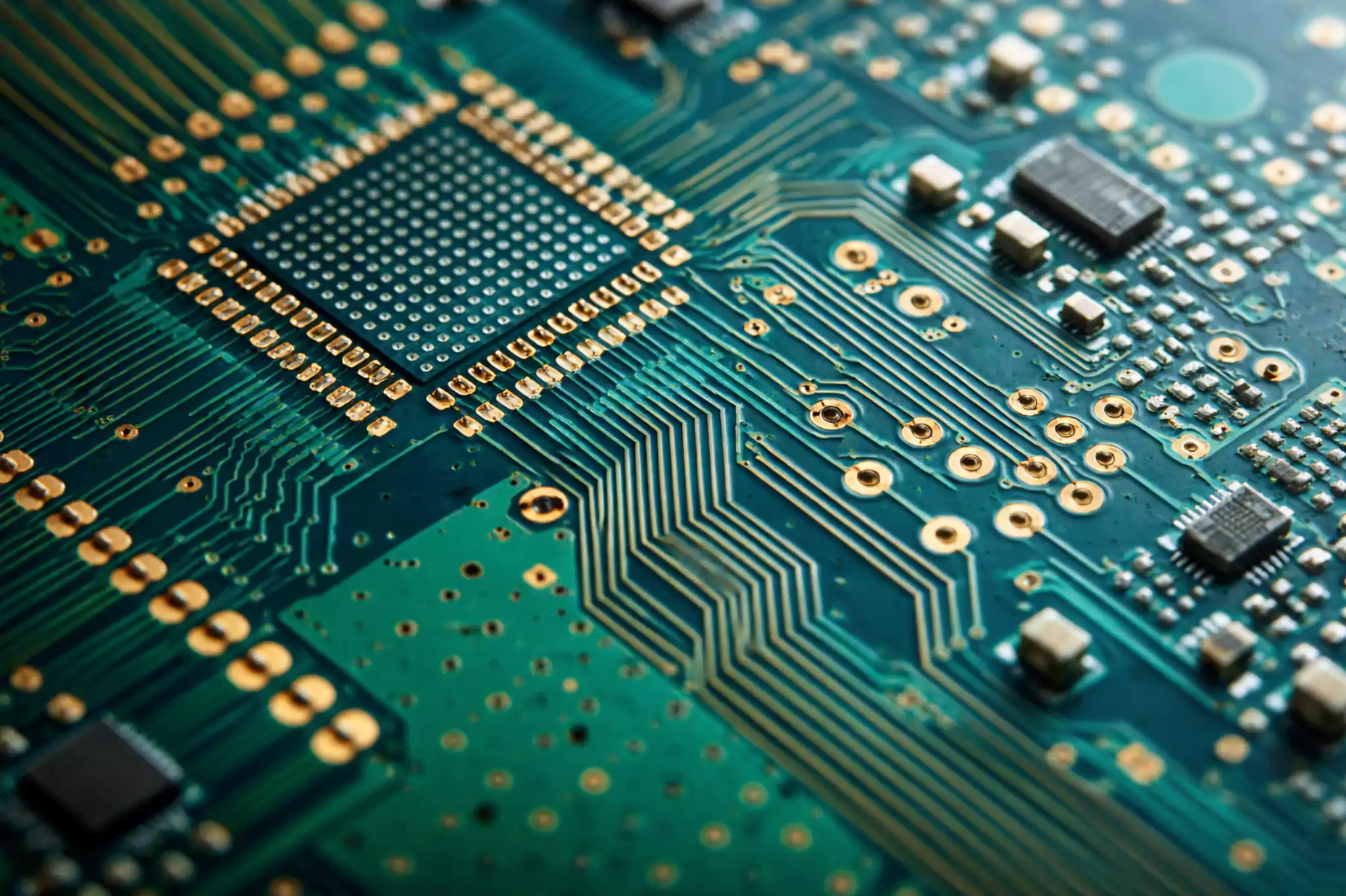

When you’re developing new hardware, a PCB prototype board is where every great product begins. It’s the bridge between a breadboard concept and a manufacturable circuit that can survive real-world testing. Modern prototype PCBs let engineers verify electrical performance, mechanical fit, and assembly reliability before committing to mass production.
At Fast Turn PCB, prototypes start from just one piece, with 24- to 72-hour turnaround and direct engineer support—so you can validate ideas and launch products faster. Now, let's clarify what sets a prototype PCB apart from other circuit-building methods.
What Is a PCB Prototype Board —and How It Differs from Breadboards & Perfboards
A PCB prototype board is a low-quantity printed circuit used to test designs before mass production. Unlike breadboards or perfboards, which use friction-fit contacts or hand-soldered wires, a prototype PCB features real copper traces and plated-through holes created from CAD files (Gerber format).
Breadboards are great for low-frequency, low-current circuits or educational use, but they introduce parasitic capacitance, loose connections, and noise. Perfboards or stripboards improve durability, but still can’t handle controlled impedance or dense SMD packages.
A custom prototype PCB replicates production board features—layer stack-up, ground planes, via types—enabling realistic tests of signal integrity, thermal behavior, and assembly yield.
Prototyping Options at a Glance
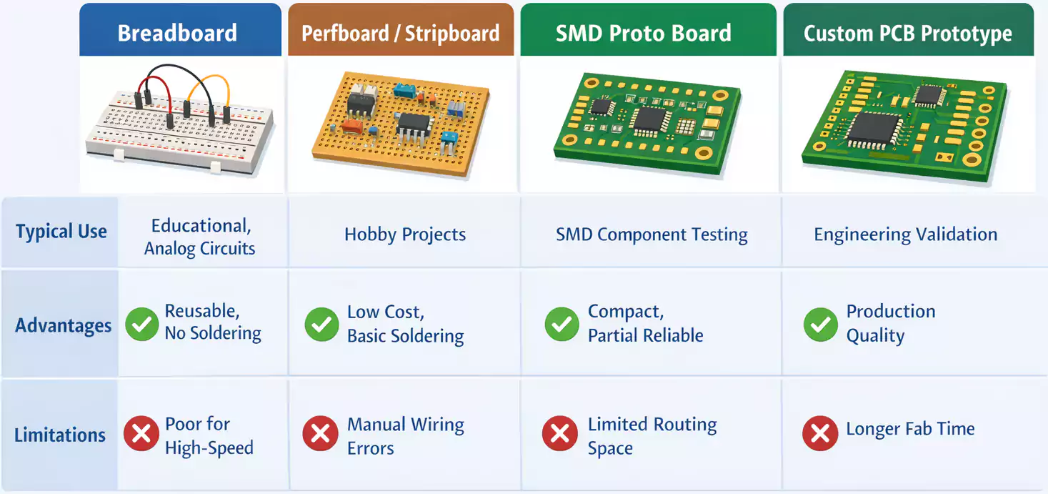
| Breadboard | Educational, analog circuits | Reusable, no soldering | Poor high-speed performance |
| Stripboard / Perfboard | Hobby projects | Low cost, basic soldering | Manual wiring errors |
| SMD Proto Board | Early SMD evaluation | Compact, partial reliability | Limited routing freedom |
| Custom PCB Prototype | Engineering validation | Real production quality | Requires fabrication time |
For signal speed, miniaturization, or reliability, upgrading from perfboard to a real PCB prototype is essential.
When to Move from Breadboard to a Custom Prototype PCB
Transitioning to a fabricated PCB becomes essential when:
- High-speed or RF signals are affected by breadboard parasitics.
- Ground and power integrity are critical to EMI/EMC compliance.
- The design must fit the mechanical enclosures or connectors precisely.
- Reliability and repeatability are required for testing or certification.
Fast Turn PCB delivers ±5% (optional ±10%) impedance control and ±0.1 mm accuracy, ensuring prototypes match production hardware—even for USB 3.0, PCIe, or RF designs.
Rapid Prototyping PCB Assembly Workflow
A smooth, rapid prototyping PCB assembly process transforms design files into functional hardware in days, not weeks.
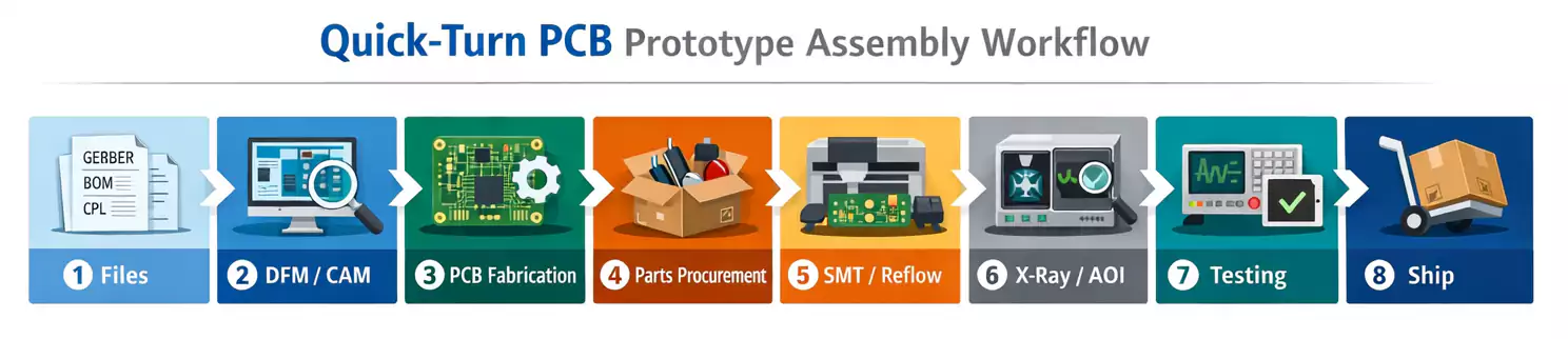
Here’s the standard quick-turn workflow:
- File Preparation — Gerber files, stack-up info, drill data, BOM, and pick-and-place (CPL).
- DFM Review (CAM) — Engineers check manufacturability: trace widths, drill-to-copper, solder mask openings.
- PCB Fabrication — Layer imaging, etching, lamination, solder mask, and surface finish (HASL, ENIG, OSP).
- Parts Procurement — Components sourced from verified distributors or customer-supplied kits.
- SMT Assembly — Automated stencil printing, pick-and-place, reflow soldering, AOI inspection.
- Testing & Shipment — Functional or in-circuit tests (ICT), packaging, and fast delivery.
Fast Turn PCB provides 24-hour bare-board builds, 48-72 hour quick-turns, and all-in-one fabrication, sourcing, assembly, and testing—streamlining your project under one roof.
DFM/DFA Checklist for First-Pass Success
Use this condensed list before submitting files:
- Maintain minimum trace/space per manufacturer’s capability (e.g., 3/3 mil).
- Keep annular rings ≥ 5 mil for reliable plating.
- Define solder-mask expansion +3 mil around pads.
- Add panel rails + tooling holes for SMT handling.
- Verify silkscreen orientation and readability.
- Ensure BOM and placement files match the design reference.
- Flag alternate parts for supply flexibility (AVL).
- Plan for X-ray or functional test points if needed.
Fast Turn PCB engineers perform instant DFM review on every order, minimizing iteration cycles and ensuring your first prototype powers up correctly.
In-House vs. PCB Prototyping Machine — Which Makes Sense in 2026
Some labs consider buying a PCB prototyping machine—such as a desktop CNC router, UV exposure unit, or small reflow oven—to fabricate boards internally. While this can work for simple single- or double-layer designs, hidden costs quickly add up:
| Upfront Cost | High (machines + chemicals) | None |
| Learning Curve | Steep | Zero |
| Accuracy | Limited registration | ±0.1 mm (CAM-controlled) |
| Multilayer Capability | 1–2 layers | Up to 12+ layers |
| Reliability | Manual process | IPC-A-600/610 Class 2+ |
| Lead-Time | 1–2 days per board | 24–72 h including assembly |
For hobby use or educational projects, in-house prototyping may suffice.
But for HDI, impedance-controlled, rigid-flex, or RF designs, outsourcing to a quick-turn PCB manufacturer like Fast Turn PCB ensures professional-quality results and a predictable turnaround.
Cost & Lead-Time Benchmarks You Can Expect
Prototype pricing scales with complexity rather than volume. Typical turnaround tiers:
| Barebone 24 h | 1 day | Electrical validation only |
| Standard Quick-Turn 48–72 h | 2–3 days | Functional testing, demo boards |
| Economy 5–7 Days | Week | Cost-sensitive trials |
| With Assembly | +1–2 days | Ready-to-test prototypes |
Lead time increases with additional layers, impedance control, fine traces, or special materials (Rogers, polyimide, heavy copper).
Fast Turn PCB manages all fabrication and assembly in-house, reducing lead times from approval to shipment.
How to Choose a Prototype PCB Manufacturer (10-Point Scorecard)
Selecting the right partner is crucial for on-time, functional prototypes. Evaluate manufacturers by these criteria:
- Engineering Responsiveness – Dedicated project engineer for real-time communication.
- DFM Capability – Automated file checks and manual CAM review.
- Manufacturing Limits – Minimum 3 / 3 mil trace/space, 0.1 mm via holes, ±5% impedance control.
- Material Range – FR-4, polyimide, Rogers, aluminum, heavy copper.
- Quality Certifications – ISO 9001, IPC Class 2 & 3.
- Traceability – Lot tracking and serialization.
- Integrated Assembly – Fabrication + SMT + Testing.
- On-Time Performance – Proven quick-turn reliability.
- Online Portal & Document Handling – Easy quote uploads, version control.
- Technical Support – Design assistance and feedback for future revisions.
Fast Turn PCB checks all ten boxes with combined PCB + PCBA manufacturing, over 350 employees, and experience serving global clients across medical, automotive, and IoT industries.
From Prototype to Low-Volume Build — De-Risk Your First 100 Units
A successful prototype is only the first step. The next challenge is scaling to low-volume PCB prototypes for pilot testing or pre-production runs.
Best practices:
- Freeze the BOM after validation; define approved alternates for supply stability.
- Adjust stencil apertures and reflow profiles for consistent solder joints.
- Reuse test jigs and fixtures to lower NPI cost.
- Apply statistical sampling and failure analysis to refine yield before ramp-up.
Fast Turn PCB supports small-batch assembly and functional testing, bridging your prototype to market-ready hardware.
Frequently Asked Questions
1. What’s the difference between a prototype PCB and a production PCB?
Prototype PCBs validate design intent and manufacturability; production boards focus on cost optimization and volume yield. Materials and stack-ups are often identical—the difference lies in quantity and test depth.
2. How fast can I get quick-turn PCB prototypes with assembly?
Standard lead time is 48–72 hours, with 24-hour bare-board options when files are DFM-ready.
3. What design files do I need to submit?
Gerber (RS-274X or ODB++), drill file, stack-up note, BOM (Excel/CSV), pick-and-place file (CPL), and assembly drawing with polarity and reference designators.
4. How can I ensure impedance and stack-up accuracy in prototypes?
Share your target impedance and differential pair geometry during quoting. Fast Turn PCB maintains ±5% impedance tolerance using verified material data and impedance coupons.
Get Your Prototype Built Fast
Whether you need one board for engineering validation or 100 for pilot testing, Fast Turn PCB delivers quick-turn PCB prototypes and rapid prototyping PCB assembly that meet professional production standards.
Upload your Gerber, BOM, and CPL files today for a free DFM review and get your assembled prototypes shipped in as little as 48–120 hours—with a dedicated engineer guiding you from design to delivery.
