


When space is limited and reliability is non-negotiable, Rigid Flex PCB offer the ideal bridge between rigid and flexible circuit technologies. These hybrid boards integrate FR-4 and polyimide substrates into a single structure, enabling three-dimensional routing while eliminating connectors and cables, which often cause mechanical or electrical failures.
This guide explains what rigid-flex PCBs are, their advantages, common multilayer stackups, design-for-manufacturability (DFM) rules, step-by-step fabrication, cost factors, and how to choose the right manufacturer.
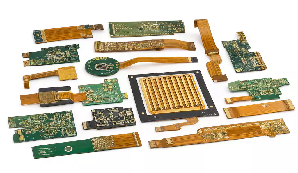
What Is a Rigid Flex PCB?
A Rigid Flex PCB combines rigid layers—typically made from FR-4 laminate—with one or more flexible layers made from polyimide (PI) film.
The rigid sections support components and provide mechanical strength, while the flexible layers bend or fold to connect different rigid areas.
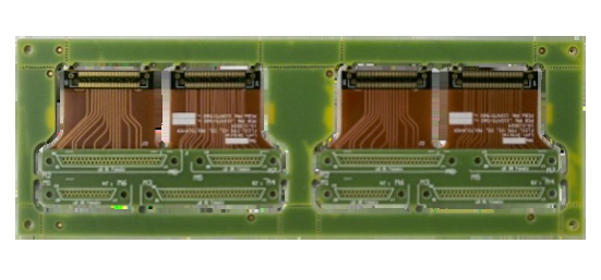
Unlike traditional rigid boards connected by cables or connectors, a rigid-flex design forms a continuous circuit. This integrated structure increases reliability, reduces assembly time, and saves both space and weight—critical in today’s compact, high-performance electronics.
Rigid-flex boards are used in medical devices, aerospace and defense electronics, cameras, wearable devices, automotive sensors, and industrial control systems.
Key Advantages and Applications
Why engineers choose rigid-flex over standard PCBs:
- Space and weight reduction – Combines multiple boards and connectors into one integrated unit.
- Higher reliability – Eliminates solder joints, connectors, and cables prone to vibration and fatigue.
- Improved electrical performance – Controlled impedance and shorter interconnections reduce EMI and signal loss.
- Ease of assembly – No manual cable routing or connector mating; simplifies testing and final assembly.
- Design flexibility – Allows folding, stacking, or wrapping to fit 3D enclosures.
These advantages make rigid-flex circuits ideal for high-reliability applications such as aerospace controls, medical imaging systems, military communication devices, and modern consumer products where every millimeter counts.
Materials and Bend-Radius Fundamentals
A high-quality rigid flex PCB depends on the right base materials and proper bending design.
Substrates
- Rigid sections use FR-4 epoxy glass laminates.
- Flexible sections use polyimide (PI) film—either adhesiveless PI for better flexibility or adhesive-based PI for cost-sensitive builds.
Copper Foil
- Rolled-annealed (RA) copper is preferred for flex zones due to its superior ductility.
- Electrodeposited (ED) copper can be used for static or limited-bend applications.
At Fast Turn PCB, typical finished copper thicknesses are:
- Flex areas: 0.5–2 oz
- Rigid areas: 1–4 oz
Coverlay and Stiffeners
- Coverlay replaces the solder mask on flex layers, protecting traces and defining pad openings.
- Stiffeners (FR-4 or polyimide) strengthen connector zones or SMT areas to prevent warping.
Bend-Radius Guidelines
- For static bends, radius ≥ 10× the total flex thickness.
- For dynamic bends, radius ≥ 20× thickness.
Always route traces perpendicular to the bend and use curved transitions instead of sharp corners.
Common Multilayer Stackups
Rigid-flex boards range from simple 2-layer flex bridges to complex multilayer systems with more than 20 layers.
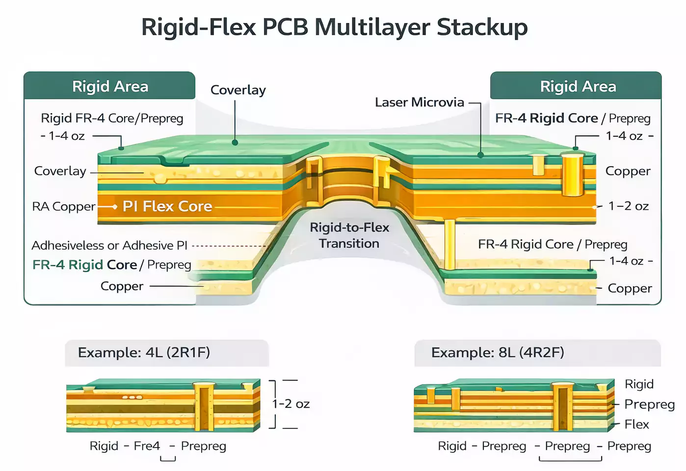
Typical Stackup Examples
- 4-Layer (2R1F): Basic configuration for connecting two rigid sections via a single flex core.
- 6–8-Layer (4R2F): Dual or symmetric flex cores centered in the stackup for balanced bending; used in folding assemblies.
- 10–12-Layer (6R2F4): High-speed or RF applications with dedicated reference planes for impedance control and EMI shielding.
- 20-Layer+ (Bookbinder construction): Advanced aerospace or defense systems requiring sequential lamination and multiple flex zones.
Balanced construction and symmetric placement of flexible layers reduce warpage and mechanical stress during lamination and operation.
DFM Design Rules for Rigid-Flex
Designing for manufacturability (DFM) is essential to ensure high yield and long-term reliability.
In the Flex Area
- Keep traces perpendicular to the bend line.
- Avoid vias, components, and sharp 90° corners.
- Use curved traces and teardrop pads.
- Employ cross-hatched or open copper planes to distribute strain.
- Maintain uniform trace distribution to prevent stress concentration.
At the Rigid-to-Flex Transition
- Use staggered step-down transitions instead of abrupt thickness changes.
- Move vias and through-holes at least 1 mm away from the flex boundary.
- Apply coverlay relief with rounded openings.
- Add strain-relief features or fillets.
Assembly Considerations
- Avoid placing components within the bend region.
- Include tooling holes and alignment fiducials.
- Define test points in rigid areas for electrical verification.
- Submit Gerber, stackup, impedance, and BOM files for DFM review before fabrication.
Fast Turn PCB offers free DFM and stackup evaluation, ensuring your rigid-flex design is manufacturable the first time.
Manufacturing Process & Quality Control
Rigid flex PCB fabrication combines the complexity of both rigid multilayer and flexible circuits.
Here’s how it’s typically done at Fast Turn PCB:
- Material Preparation – Cut and clean FR-4 and PI films.
- Inner-Layer Imaging & Etching – Define traces and ground planes.
- Lamination – Combine rigid and flexible layers under heat and pressure.
- Drilling – Use mechanical and laser micro-via drilling (as small as 0.10 mm).
- Plating & Via Metallization – Ensure conductivity through all layers.
- Outer-Layer Imaging / Etching – Define external circuitry.
- Surface Finish – ENIG, HASL (lead-free), OSP, immersion silver or tin, or Ni-Pd-Au.
- Coverlay & Stiffener Application – Add mechanical protection and rigidity.
- Routing & Profiling – CNC or laser cutting to final dimensions (up to 620 × 500 mm).
- Testing & Inspection – 100 % E-test, AOI, and X-ray inspection for quality assurance.
Manufacturing Challenges
- Debris and smear removal on mixed materials (FR-4 + PI).
- Precise registration during sequential lamination.
- Controlling interlayer stress to avoid delamination or wrinkles in flex zones.
Fast Turn PCB controls these variables through precision laser drilling, vacuum lamination presses, and AOI/X-ray inspection, and is supported by ISO 9001, UL, and RoHS certifications.
Cost & Lead-Time Factors
Rigid flex PCB require more process steps and materials than standard boards, so understanding cost drivers helps with optimization.
Main Cost Drivers
- Number of layers and flexible areas
- Length and count of flex zones
- Microvia and buried-via structures
- Copper thickness and coverlay openings
- Impedance control and testing requirements
- Yield rate (scrap due to mis-registration or delamination)
Optimization Tips
- Combine flex zones when possible.
- Simplify layer count and avoid unnecessary dynamic bends.
- Use standardized panel sizes and outlines.
- Engage your fabricator early to collaborate on DFM.
Typical Lead Time
At Fast Turn PCB, build times range from 7 to 20 days, depending on layer count, complexity, and quantity. Quick-turn prototyping and volume production are both supported under one roof.
How to Choose a Flex-Rigid Manufacturer
Selecting the right partner is critical for project success. Use these benchmarks as your checklist.
Key Capability Parameters (Fast Turn PCB Example)
| Max Layers | Up to 26 layers |
| Min Trace/Space | 0.065 / 0.065 mm |
| Min Drill / Pad | 0.10 mm / 0.35 mm |
| Drill Accuracy | ± 0.05 mm |
| PTH Tolerance | ± 0.05 mm |
| Max Panel Size | 620 × 500 mm |
| Finished Thickness | 0.25 – 6.0 mm |
| Surface Finishes | ENIG, HASL (LF), OSP, Immersion Silver/Tin, Ni-Pd-Au |
Quality and Compliance
Look for ISO 9001, UL, and RoHS certifications. For aerospace, medical, or military projects, ensure IPC-6013 Class 3 standards and traceable quality documentation.
Engineering & Support
A good supplier provides:
- One-on-one engineering review
- Stackup and impedance consultation
- File compatibility (Gerber, ODB++, IPC-2581)
- Rapid, transparent communication from quotation to shipment
Fast Turn PCB provides exactly this level of support—helping customers move from prototype to mass production without redesign delays.
Frequently Asked Questions (FAQ)
1. What is the minimum bend radius for rigid flex PCB?
For static bends, use ≥ 10× the flex thickness; for dynamic, ≥ 20×. Always route traces perpendicular to the bend.
2. Can differential pairs run through flex areas?
Yes, if impedance is controlled and a continuous return path is maintained using reference planes or mesh copper.
3. When should stiffeners be used?
At connector pads, SMT component areas, or where mechanical reinforcement is required.
4. Can vias be placed in the flex zone?
Avoid in dynamic flex areas. If unavoidable, keep them away from the bend center and use teardrop pads with larger annular rings.
5. What’s the typical lead time for multilayer rigid-flex boards?
Depending on layer count and complexity, lead time ranges from 7 to 20 days at Fast Turn PCB.
Conclusion
Rigid flex PCB delivers the ultimate combination of miniaturization, reliability, and design freedom.
By merging flexible and rigid technologies, they reduce interconnects, improve electrical performance, and enable compact 3D architectures.
With Fast Turn PCB’s 26-layer capability, precision micro-via drilling, full in-house lamination, and 7–20 day build times, you can take your rigid-flex design from prototype to production with confidence.
