

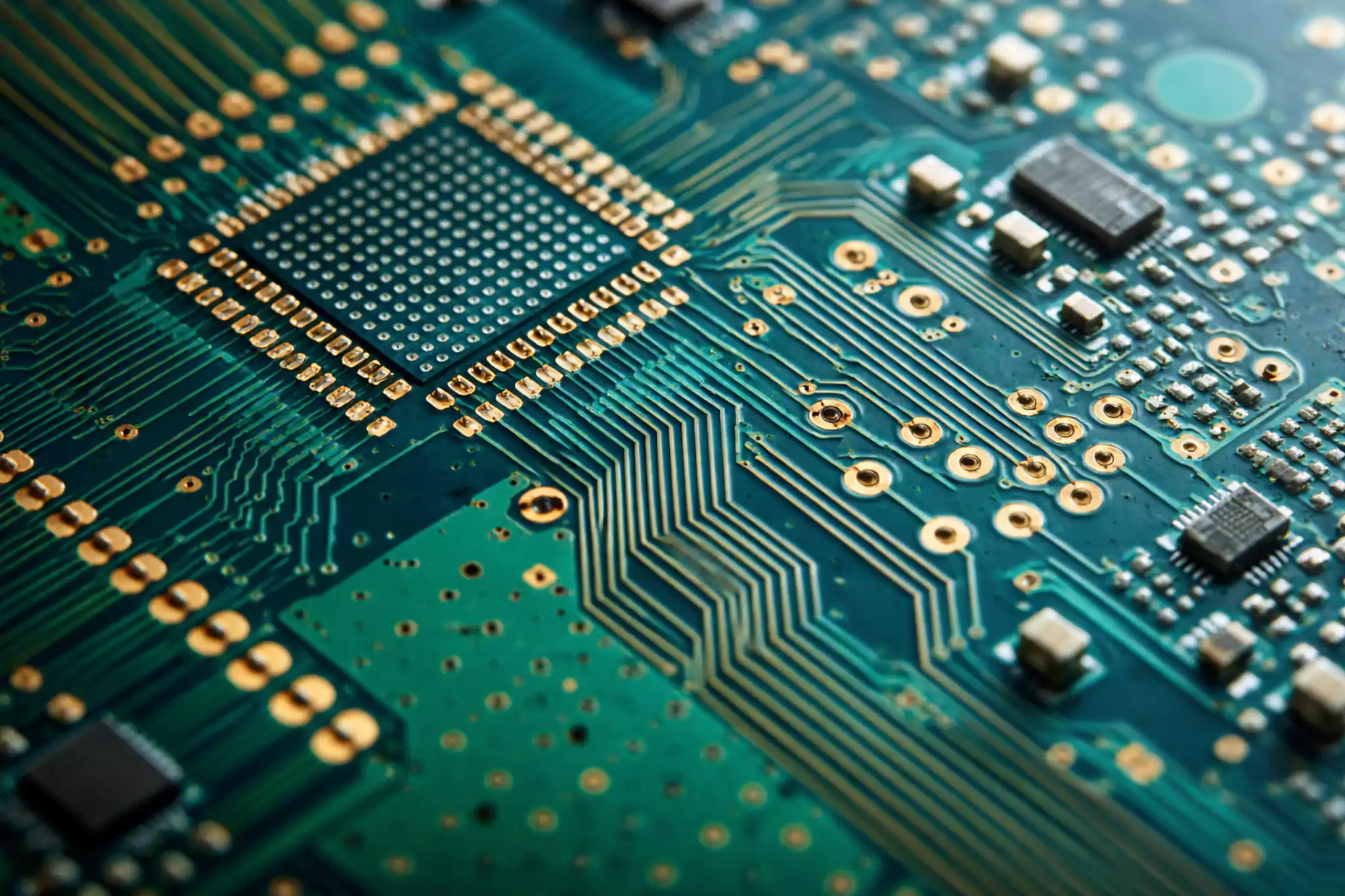

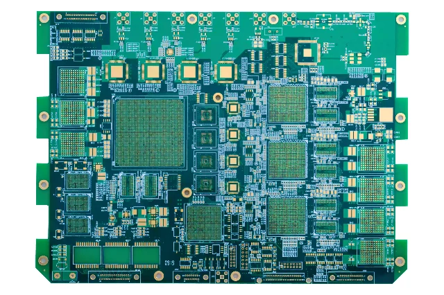
When every square millimeter of a PCB matters, HDI Circuit Boards are the only practical solution. They allow engineers to route more signals, reduce form factor, and maintain signal integrity in today’s compact, high-speed electronics.
Fast Turn PCB offers full HDI PCB manufacturing — including laser drilling, sequential lamination, via filling, and impedance control. Featuring 2.5/2.5 mil line/space, 100 µm microvias, up to 18 HDI build-up layers, and 24- to 48-hour prototype turnaround, it provides a one-stop service for high-density designs.
What are HDI Circuit Boards?
An HDI (High-Density Interconnect) PCB is designed to pack more routing and interconnections into the same area compared with conventional multilayer boards. It achieves this through:
- Blind and buried vias instead of full through-holes.
- Laser-drilled microvias as small as 100 µm in diameter.
- Fine line widths and spaces — down to 2.5/2.5 mil.
- Sequential lamination (SBU) to add build-up layers selectively.
These technologies shorten trace lengths, lower parasitic inductance, and improve power integrity — essential for 5G, AI servers, automotive control modules, and wearables.
Fast Turn PCB integrates blind/buried vias, laser microvias, via-in-pad, and via filling within a unified, tightly controlled process for high reliability from prototype to mass production.
HDI Stack-Ups That Actually Ship
In HDI fabrication, stack-up design defines performance, manufacturability, and cost. Fast Turn PCB routinely produces:

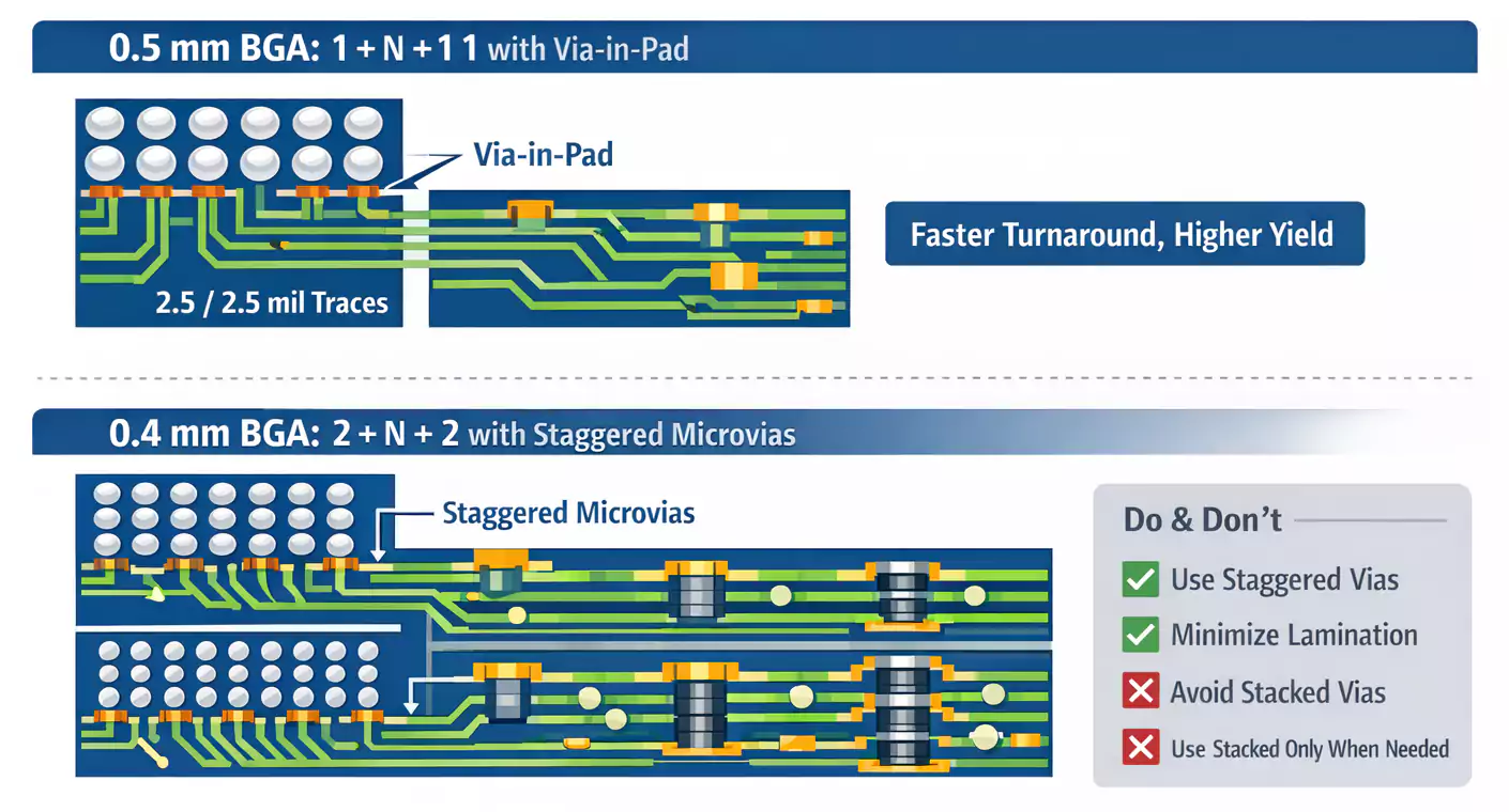
- 1 + N + 1 structures — one microvia layer per side, ideal for ≥ 0.5 mm BGA breakout with excellent yield and quick turnaround.
- 2 + N + 2 — two HDI layers per side, used for 0.4 mm-pitch BGAs that require more routing channels.
- Up to 18 build-up layers (total 20) for advanced telecom, automotive, and aerospace systems.
Each type uses a different sequence of laser-drilled layers and lamination steps. A clear understanding of the trade-offs helps designers minimize press cycles and control cost without sacrificing reliability.
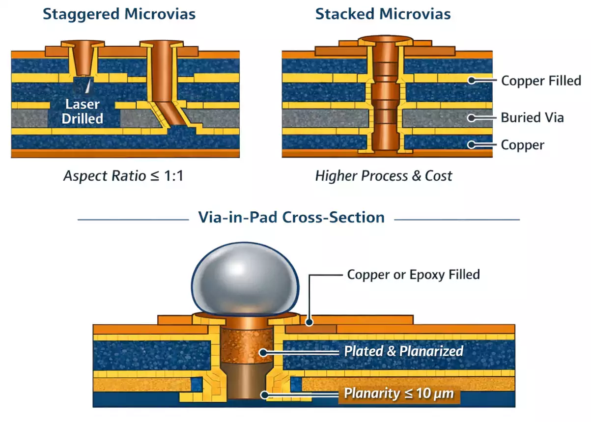
Microvias, Blind/Buried Vias & Via-in-Pad
Microvias are the foundation of every HDI stack-up. These laser-drilled holes (≈ 100 µm) connect only one layer at a time, keeping aspect ratio ≤ 1:1 for strong copper plating and minimal stress.
Blind vias connect outer layers to inner ones; buried vias connect internal layers only. Fast Turn PCB supports microvias and blind/buried vias in the 0.15–0.30 mm range (± 5 µm tolerance), optimized for controlled depth and clean hole walls.
For very tight BGA layouts, via-in-pad structures are used — microvias drilled directly into component pads, then filled and plated to create a flat surface for reflow soldering. Fast Turn PCB applies copper or epoxy filling with surface planarity ≤ 10 µm, ensuring void-free connections and reliable assembly.
Design Rules That Balance Yield & Cost
The most successful HDI designs stay within stable, repeatable process windows. Fast Turn PCB recommends the following manufacturable ranges:
- Minimum trace/space: 2.5 / 2.5 mil (0.063 / 0.063 mm).
- Minimum plated through-hole: 0.15 mm (6 mil) finished.
- Microvia diameter/pad: 100 µm / 200 µm.
- Controlled impedance tolerance: ± 5 Ω or ± 10 %.
- Copper thickness: 1 – 6 oz outer/inner.
- Board thickness: 0.4 – 3.2 mm.
Material options include high-Tg FR-4 and halogen-free laminates for automotive and industrial reliability requirements. Mixed dielectric stack-ups (FR-4 + low-loss cores) are also available for high-speed designs.
Routing guideline:
- For 0.5 mm BGA, use a 1 + N + 1 stack-up with via-in-pad.
- For 0.4 mm and smaller, move to 2 + N + 2 and use staggered or stacked microvias.
Manufacturing Snapshot
Every HDI Circuit Boards at Fast Turn PCB goes through a precisely controlled process chain:
- Sequential lamination (SBU): Multiple press cycles build new microvia layers while maintaining layer-to-layer registration within ± 25 µm.
- Laser drilling: CO₂/UV laser systems produce 100 µm vias with smooth walls and accurate depth control.
- Via filling and copper plating: Advanced plating ensures complete via fill and even copper distribution; surface flatness ≤ 10 µm.
- LDI imaging and fine-line etching: Laser direct imaging achieves sub-3 mil traces with high yield.
- AOI, X-ray, and cross-section analysis: Each production batch includes inspection reports for trace width, via fill, copper thickness, and impedance validation.
This closed-loop quality system guarantees consistent stack-ups and repeatable impedance results from prototype to volume builds.
Applications
HDI technology enables today’s high-performance electronics across industries:
- Smartphones & wearables: Compact PCBs with any-layer interconnects and fine-pitch BGAs.
- Automotive electronics: ADAS, infotainment, radar, and control modules demanding high reliability.
- Servers & AI accelerators: Dense multilayer interconnects with controlled impedance for high-speed differential pairs.
- Medical & aerospace: Lightweight yet robust boards with stable thermal expansion characteristics.
Fast Turn PCB supports all these sectors with an integrated workflow: DFM review, rapid prototyping, ramp-to-production, full testing, and traceability.
How to Choose an HDI PCB Manufacturer
Selecting the right manufacturing partner is crucial for HDI success. Here’s what to verify before awarding your next project:
- Capability data: Confirm the factory can handle 2.5/2.5 mil lines, 100 µm microvias, and 0.15 mm plated through-holes in production, not just in lab samples.
- Stack-up experience: Request build records for 1 + N + 1, 2 + N + 2, or higher (up to 18 HDI / 20 total layers).
- Quality control: Request AOI, X-ray, cross-section, and impedance test reports for each batch.
- Turnaround & NPI support: Evaluate if the manufacturer offers 24- to 48-hour prototypes and rapid engineering feedback.
- Supply-chain and reliability standards: Look for ISO 9001, IPC-A-600/6012, and RoHS compliance.
Fast Turn PCB checks every box — providing transparent reports, responsive engineering, and dependable logistics.
👉 Learn more about our HDI PCB Manufacturer capabilities, explore High Density Interconnect PCB Fabrication details, or contact your dedicated Microvia PCB Manufacturer engineer for a quote.
HDI FAQ
1. What microvia sizes are typical for HDI PCBs?
Laser-drilled microvias of ≈ 100 µm (4 mil) with 200 µm pads are standard. Aspect ratio is kept at or below 1:1 for reliable copper plating.
2. What’s your smallest line and space?
Fast Turn PCB supports 2.5/2.5 mil (0.063 mm) for stable mass-production yields with ±10% impedance tolerance.
3. How fast can HDI prototypes be built?
Typical turnaround is 24–48 hours for small-batch HDI prototypes, including DFM review and testing.
4. What stack-ups are available?
Common options include 1 + N + 1 and 2 + N + 2 with up to 18 HDI build-up layers or 20 total layers, depending on design complexity.
Conclusion
HDI circuit boards are the backbone of modern miniaturized electronics, from smartphones to satellites. Success depends on both design discipline and manufacturing capability.
Fast Turn PCB combines engineering expertise, precision equipment, and responsive service to accelerate and improve the reliability of HDI fabrication. Whether you need a 4-layer 1 + N + 1 prototype or an 18-layer production stack-up with filled microvias and via-in-pad, our engineers will guide you from concept to shipment — ensuring your boards perform the first time.
