

Resin content is often discussed only in relation to dielectric constant. In real PCB manufacturing, however, it also affects Z-axis expansion, CAF resistance, board flatness, and process stability.These effects become more critical in multilayer boards and thin inner layers, where both reliability and manufacturability matter.
How Resin Content Affects Laminate Performance
For the same dielectric thickness, multiple combinations of glass fabric and resin content may be possible. Resin content should be viewed as a multi-function parameter that influences electrical, mechanical, and manufacturing behavior.

1. Benefits of Lower Resin Content
Lower resin content generally provides:
- Lower Z-axis thermal expansion
- Improved plated through-hole reliability
- Better dimensional stability
- Reduced warpage
- More stable dielectric thickness
These advantages are important in industrial, automotive, and communication PCBs. Lower Z-axis expansion reduces stress during thermal cycling, thereby extending product life.
2. Electrical Benefits of Higher Resin Content
Higher resin content also has benefits. Increasing the resin ratio lowers the dielectric constant, improving impedance control and high-speed signal performance.
For high-speed digital or RF boards, electrical performance may be prioritized, even if manufacturing becomes more challenging. This is a common and accepted trade-off in advanced designs.
3. Minimum Resin Content Requirements
Resin content cannot be reduced without limits. The resin must fully wet the glass fibers and prevent voids or dry spots inside the laminate.
If resin content is too low, problems may occur, including:
- CAF (Conductive Anodic Filament) growth
- Poor thermal reliability
- Reduced long-term durability
Industry experience shows that resin starvation and exposed glass fibers are major contributors to CAF failures. Each glass style has an optimal resin content range that balances electrical, mechanical, and reliability needs.
Flatness and Mechanical Strength
Flatness and stiffness are critical during PCB manufacturing, especially when producing thin inner layers. Boards must pass through automated equipment without bending or damage.
1. Why Flatness Matters
If a laminate curls or bends, it can jam conveyors or damage equipment during processing. Thin inner layers with copper patterns are especially vulnerable. As laminate thickness decreases, sensitivity to warpage increases.
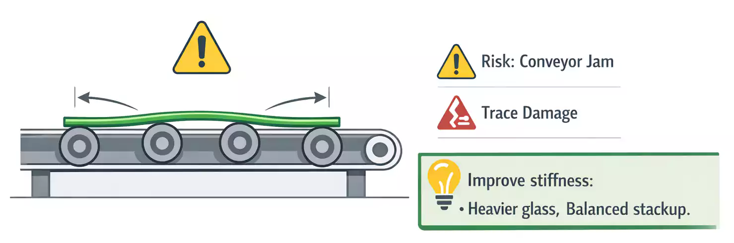
2. Improving Bending Strength
Manufacturers may improve stiffness by increasing glass content or using heavier glass fabrics. This helps resist bending but must be balanced against resin content and electrical requirements.
3. Symmetry and Warpage Control
Symmetrical or balanced stackups help reduce warpage by balancing thermal and mechanical stress. Asymmetrical structures are more likely to bow or twist.
For example, a 0.008-inch dielectric layer may use:
- One sheet of 7628
- One sheet of 2313 plus one sheet of 2116 (asymmetrical)
- Two sheets of 2116
The asymmetrical option tends to warp more, but warpage is only one design factor. Final decisions must also consider thickness control, electrical performance, and mechanical reliability.
Conclusion
From a PCB manufacturer’s perspective, laminate design is always a balance. Electrical performance, mechanical reliability, and stable production must all be considered. Understanding these trade-offs early helps avoid cost increases, yield loss, and schedule delays later in fabrication.
