

On a printed circuit board (PCB), the thin copper lines running across it are called traces.
Each trace carries signals or power between components, and its design directly impacts circuit performance.
This guide explains what a PCB trace is, how to size it correctly, how standards like IPC-2152 help you, and what tools, such as the trace width calculator, can do for you.

What Is a PCB Trace?
A PCB trace is a flat, narrow copper path on a circuit board.
It connects components, allowing current to flow between them like wires, but in a compact, printed form.
Every trace has a few key parameters:
- Width: how wide the copper line is.
- Spacing: the distance between neighbouring traces.
- Copper thickness: how thick the copper layer is (usually measured in ounces per square foot).
- Length: Longer traces add resistance and voltage drop.
- Impedance: In high-speed circuits, this defines how signals travel.
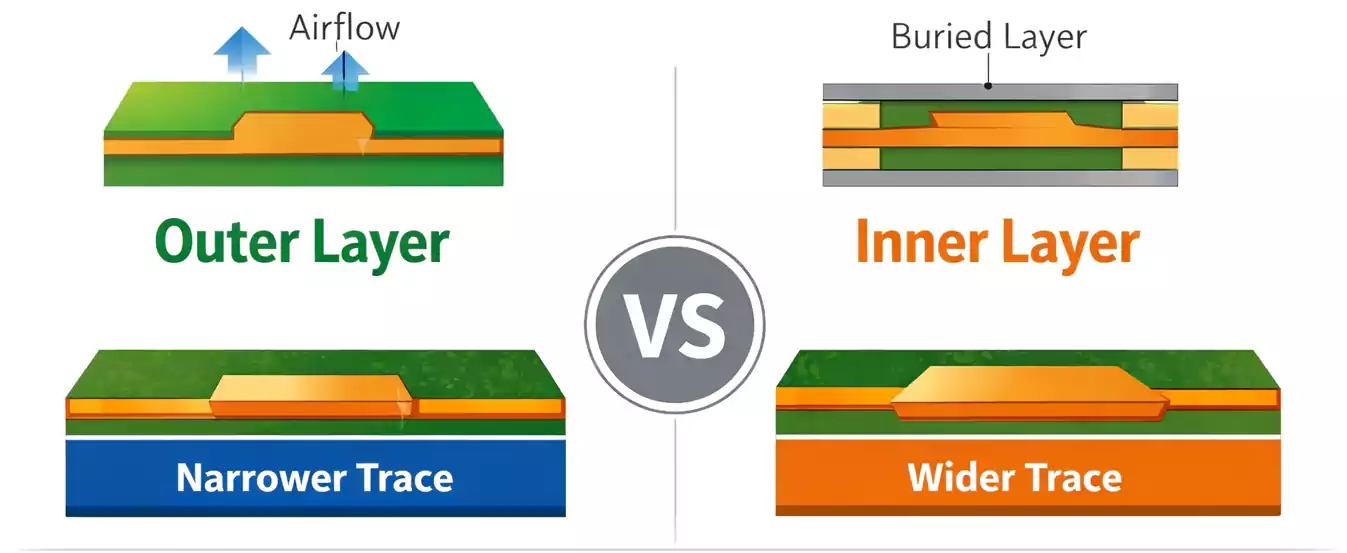
Traces can be located in the outer layers (exposed to air and easy to cool) or in the inner layers (buried between dielectric materials).
Because inner layers hold heat more easily, they carry less current for the same width.
What Determines PCB Trace Width?
1. Current and Temperature Rise
The most important factors are the current the trace will carry, and the temperature rise you can accept.
If the trace gets too hot, the resistance increases, potentially damaging the board.
The outer layers cool faster due to airflow, while the inner layers require wider traces to carry the same current.
2. Copper Thickness
PCB copper is typically 1 oz/ft² (≈ 35 µm thick).
Thicker copper, such as 2 oz or 3 oz, allows narrower traces for the same current.
3. Trace Length and Voltage Drop
The longer the trace, the greater its resistance.
This can cause voltage drop and power loss, especially in power lines or ground networks.
4. Environment and Cooling
Encapsulation, solder mask, and airflow also influence heat dissipation.
Covered or inner traces trap more heat, so increase the width or reduce the current density.
5. Manufacturing Limits
Every PCB factory has minimum trace width and spacing rules.
Standard manufacturing allows 4–6 mil traces; HDI boards can go down to 2 mil or even less.
IPC-2221 vs. IPC-2152: Which One to Use?
Both standards define how to calculate PCB trace width, but they differ in how they do so.
IPC-2221 (Old Formula)
This older standard is based on empirical equations developed decades ago.
It gives a rough estimate but often doesn’t reflect modern materials or inner-layer conditions.
IPC-2152 (Updated & Tested)
IPC-2152 is based on real thermal testing and covers more variables, such as layer position, copper thickness, and environmental conditions.
It is more accurate and conservative, and is now the recommended reference for new designs.
How to Use a Trace Width Calculator
Online calculators make this job fast and easy.
They use IPC-2221 or IPC-2152 formulas to estimate the required width for a given current and temperature rise.
You usually need to input:
- Current (A)
- Temperature rise (°C)
- Copper thickness (oz or µm)
- Layer type (internal or external)
For example, to carry 2 A on an outer layer with 1 oz copper and 10 °C rise, the calculator might suggest a width of around 20 mil (0.5 mm).
If the same trace were on an inner layer, it would need to be about 40 mil.
High-Speed Traces and Impedance Control
In digital or RF circuits, trace width isn’t only about current — it also affects impedance.
When signals reach hundreds of MHz or several GHz, the trace behaves like a transmission line.
Microstrip and Stripline
- Microstrip: a trace on an outer layer with one side exposed to air and a ground plane underneath.
- Stripline: a trace buried between two reference planes inside the board.
The impedance depends on:
- Trace width
- Dielectric thickness
- Dielectric constant (Dk) of the material
- Copper thickness and roughness
Designers aim for controlled impedance, typically 50 Ω single-ended or 100 Ω differential for most digital buses (USB, HDMI, PCIe, etc.).
High-Current Traces and Power Delivery
Power traces and ground networks carry large currents and can heat up quickly.
Good layout keeps them short, wide, and evenly distributed.
Key Rules
- Use short, straight paths. Long or narrow routes create a voltage drop.
- Increase copper thickness. 2 oz or 3 oz copper can double the current capacity.
- Use multiple vias for current return. Parallel vias reduce resistance and improve cooling.
- Add thermal relief or copper pours. A solid copper plane spreads heat effectively.
- Avoid bottlenecks. Check the pad neck-downs or narrow corners that may overheat.
These steps improve reliability and reduce the risk of trace burnout in power supplies, motor drivers, or LED circuits.
EMC, Crosstalk & Grounding Tips
Electromagnetic compatibility (EMC) problems often start with poor trace layout.
Here are a few easy-to-follow rules:
- Keep return paths short and direct. The signal should always flow above its ground reference.
- Separate noisy and sensitive traces. Keep analogue lines away from switching regulators or clocks.
- Use guard traces only when helpful. A grounded shield trace between high-speed lines can reduce crosstalk — but only if it’s properly grounded.
- Avoid running high-speed traces over plane splits. This breaks the return path and causes EMI.
Even small geometric changes can cut noise and improve signal integrity.
Quick Reference FAQ
Q1: Why do inner layers need wider traces than outer layers?
Because inner layers can’t release heat as easily — they’re surrounded by insulating materials.
Q2: Is IPC-2152 more accurate than IPC-2221?
Yes. IPC-2152 is based on real thermal testing and provides more realistic results.
Q3: How do I estimate the width for 5 A with a 10 °C rise?
For an outer layer with 1 oz copper, you’ll need a width of around 60–70 mils. Use a calculator for the exact value.
Final Thoughts
Designing PCB traces is both an art and a science.
A trace that’s too narrow can overheat, while one that’s too wide wastes valuable board space.
By following IPC-2152 standards, checking your design with a trace width calculator, you can create boards that are safe, efficient, and ready for mass production.
Whether you’re routing a high-speed microcontroller board or a high-current power driver, good trace design remains the foundation of reliable and high-performance electronics.
