

What Is a Surface Mount PCB?
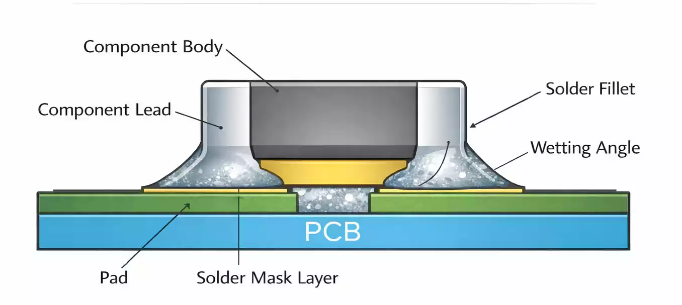
A surface-mount PCB is a printed circuit board where electronic components are soldered directly onto pads on the surface—no drilled holes required. This method is called Surface Mount Technology (SMT), and the parts are Surface-Mount Devices (SMDs).
Compared with through-hole (THT) designs, SMT allows much higher component density. Parts are smallerand lighter, and can be mounted on either side of the board.

SMT vs. THT: Which One to Choose?
The main difference between SMT and THT lies in how components are attached.
- THT (Through-Hole) parts have long leads that go through drilled holes and are soldered on the opposite side.
- SMT parts sit on pads and are soldered by reflow.
When to use SMT:
- When you need smaller boards with high circuit density.
- For automated assembly and mass production.
- When performance and signal speed matter.
When to use THT:
- For large or heavy components, like connectors or transformers.
- When high mechanical strength is required.
Often, modern products use mixed assembly: small logic circuits with SMT and power components with THT.
Surface Mount PCB Design Process
Designing an SMT board starts with clear planning. Here are the key steps:
1. Schematic and Footprints
Use standard SMD footprints from your CAD library.
Check polarity marks, pin numbers, and reference designators to prevent placement errors.
2. Component Placement
Group components by function — power, signal, and control.
Keep high-frequency, sensitive components close together.
Leave enough space for the pick-and-place machine and reflow process.
3. Routing
Use short, direct traces to reduce resistance and noise.
For high-speed signals, control impedance and keep differential pairs balanced.
For BGAs, plan fan-outs carefully and use via-in-pad designs if needed.
4. Manufacturing Details
Add fiducial marks and tooling holes for alignment.
Use panelization (V-cut or mouse-bite) for small boards to improve handling during assembly.
PCB Stencil and Solder Paste
A stencil is a thin metal sheet used to print solder paste onto pads before components are placed.
It ensures the right amount of paste goes to each pad.
1. Why Stencils Matter
Without a stencil, manual paste printing can result in either too much or too little solder, leading to defects.
2. Thickness and Aperture Design
Typical stencil thickness ranges from 0.10 to 0.15 mm.
Thinner stencils are used for small-pitch components, while thicker stencils are used for larger pads.
For fine-pitch devices like QFN or BGA, apertures are sometimes reduced slightly to avoid solder bridges.
For small parts (0402 or 0201), the stencil design helps prevent tombstoning or shifting.
3. Solder Paste Basics
Solder paste is made of metal powder and flux.
Choose the correct alloy — lead-free (SAC305) or lead-based (Sn63Pb37) — depending on requirements.
Keep pastries refrigerated and use them within their shelf life.

Surface Mount PCB Assembly Process
SMT assembly is highly automated and follows several key steps:
1. Solder Paste Printing
The stencil is placed over the PCB, and a metal squeegee spreads the solder paste evenly.
Consistent printing is critical for reliable solder joints.
2. Pick and Place
High-speed machines place components on the board according to the CAD data.
Reels, trays, or tubes feed components automatically into the machine.
3. Reflow Soldering
The loaded board passes through a reflow oven.
The temperature profile typically includes preheat, soak, reflow, and cooling stages.
Solder melts and forms solid joints between pads and leads.
4. Cleaning and Coating
If required, boards are cleaned to remove flux residues.
For harsh environments, conformal coating protects against moisture and dust.
5. Inspection and Testing
- SPI (Solder Paste Inspection) checks paste volume.
- AOI (Automated Optical Inspection) verifies placement and solder joints.
- X-ray inspection detects hidden joints in packages such as BGA or QFN.
Common SMT Defects and How to Prevent Them
Even with automation, defects can occur. Here are the most common ones:
| Tombstoning | Uneven paste or heat imbalance | Balanced pad design, correct reflow profile |
| Bridging | Too much solder or narrow spacing | Adjust stencil openings |
| Insufficient Solder | Paste volume too low | Increase aperture or paste thickness |
| Solder Balling | Flux spatter during reflow | Optimize temperature curve |
| Voids in BGA | Paste gas trapped during heating | Use proper reflow ramp-up rate |
Designing pads correctly and keeping the process under control greatly improves yield.
Electrical and Reliability Benefits of SMT
1. Better Electrical Performance
Shorter leads mean lower inductance and capacitance, reducing signal distortion.
This improves signal integrity (SI) and power integrity (PI), especially for GHz-level designs.
2. Compact and Lightweight
SMT enables smaller boards and lighter products — essential for portable devices and IoT hardware.
3. Mechanical and Thermal Reliability
Proper pad design and solder volume control ensure strong solder joints.
For power devices, using thermal vias and large copper areas improves heat dissipation.
However, repeated thermal cycling can fatigue joints, so materials and layout must be balanced.
PCB Materials and Surface Finishes for SMT
1. Base Material
For lead-free reflow, use laminates with a higher glass transition temperature (Tg) and a lower thermal expansion coefficient (CTE) — typically FR-4 rated above 170°C.
2. Surface Finishes
The surface finish affects solderability and flatness:
- ENIG (Electroless Nickel Immersion Gold): Excellent solderability, flat, good for fine-pitch components.
- Immersion Silver: Cost-effective, suitable for high-frequency signals.
- OSP (Organic Solderability Preservative): Eco-friendly and affordable for short-term use.
- HASL (Hot Air Solder Levelling): Economical but less flat, not ideal for small-pitch SMT.
3. Warpage Control
PCB warpage can cause poor solder joints.
Use symmetrical stack-up and balanced copper layers to reduce bending during reflow.
Mixed Assembly and Advanced Packages
Many products today use mixed technology — SMT and THT on the same board.
1. Typical Mixed Assembly
- SMT for signal and logic circuits
- THT for power components or connectors
2. Working with BGA and QFN
For BGA packages, fan-out design and via-in-pad are key.
For QFN, design a solid thermal pad under the chip with proper solder paste openings to avoid voids.
3. Double-Sided Reflow
When components are on both sides, place the lighter parts first and solder them on the bottom side.
The second reflow is done carefully to avoid re-melting existing joints.
Common Questions About Surface Mount PCBs
Q1: Why do BGA solder joints sometimes have voids?
Trapped gases or poor paste release can cause voids. Use optimised stencil design and controlled heating.
Q2: Which surface finish is best for SMT?
ENIG and immersion silver are popular because they provide flat, solder-friendly surfaces.
Q3: What’s the main benefit of SMT in high-speed circuits?
Shorter connections reduce parasitic effects, improving signal quality at high frequencies.
Conclusion
Surface-mount PCB technology is the backbone of modern electronics.
It allows smaller, faster, and more reliable circuit boards while reducing cost in volume production.
By following good design practices — proper layout, stencil design, and reflow control — you can achieve high-quality, high-yield assemblies for any product.
At FastTurn PCBs, we specialise in fast, reliable SMT and mixed-technology PCB fabrication.
From prototype to full production, our team ensures precision, consistency, and on-time delivery for every board.
