Производитель прототипов печатных плат
Услуги по быстрому изготовлению прототипов и серийному производству гибких печатных плат.
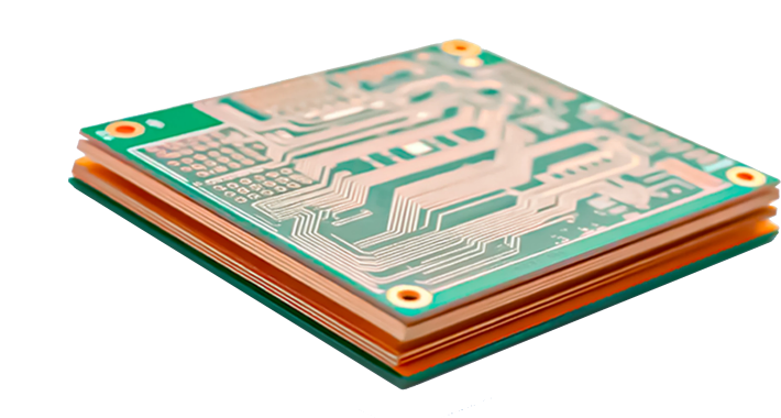
Являясь ведущим китайским поставщиком гибких печатных плат, мы специализируемся на производстве высококачественных гибких схем — от быстрого изготовления прототипов до полномасштабного производства гибких печатных плат. Загрузите ваши файлы Gerber прямо сейчас, чтобы получить быстрое и надежное коммерческое предложение.


Что такое прототипирование печатных плат?
Прототипирование печатных плат предполагает быстрое изготовление небольшой партии плат на основе проектных файлов перед началом массового производства. Это позволяет провести функциональную проверку, тестирование производительности и оценку технологических процессов. Прототипы позволяют инженерам оперативно выявлять недостатки конструкции и оптимизировать компоновку, обеспечивая безупречное крупномасштабное производство.
Почему стоит выбрать нашу услугу по изготовлению прототипов печатных плат?
Standard lead time of 5–7 business days; 3‑day expedited delivery for urgent R&D needs.
Minimum line width/spacing of 4 mil; hole sizes down to 0.2 mm; supports multilayer, flex, and HDI boards.
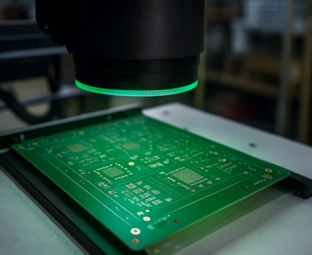
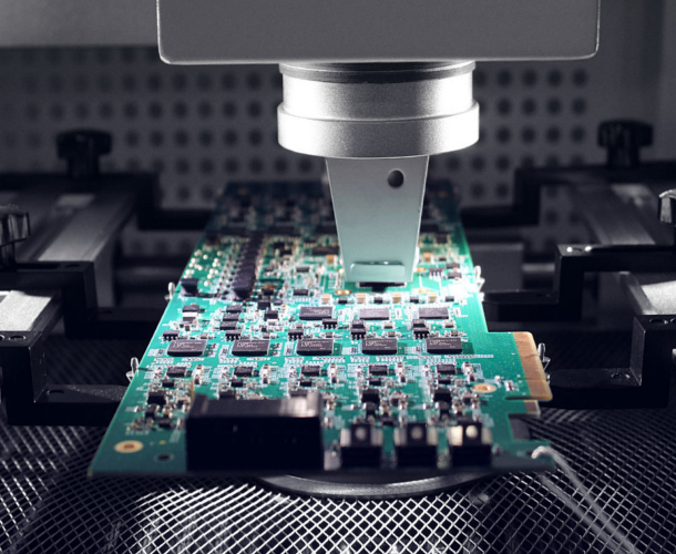
IPC-610 compliant with AOI, ICT, and X-ray inspections—100% coverage to eliminate manufacturing defects.
From prototyping and SMT assembly to stencil fabrication and DFM checks, streamlining communication and shortening project cycles.
Процесс и рабочий процесс
Шаг 1
Представление проекта
- Загрузите файлы Gerber/CAD
- Поддерживает форматы Gerber 274X, ODB++ и IPC-2581.
- Файлы автоматически архивируются с использованием уникального идентификатора проекта.
Шаг 2
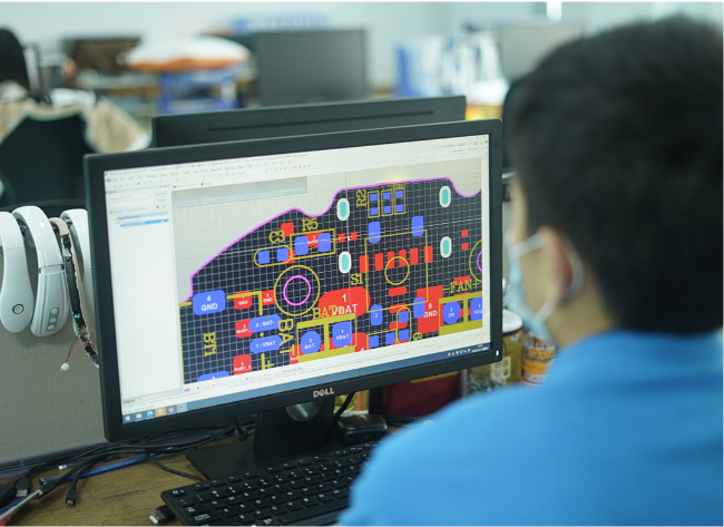
Технический обзор
- Ручная оценка в течение 2 часов.
- Основные параметры для проверки: минимальная ширина/расстояние между линиями, диаметр отверстий, размеры отверстий в паяльной маске и зазор между маской и контактными площадками.
- Предложения по оптимизации были отправлены и подтверждены по электронной почте или по телефону.
Шаг 3
Прототипирование и изготовление
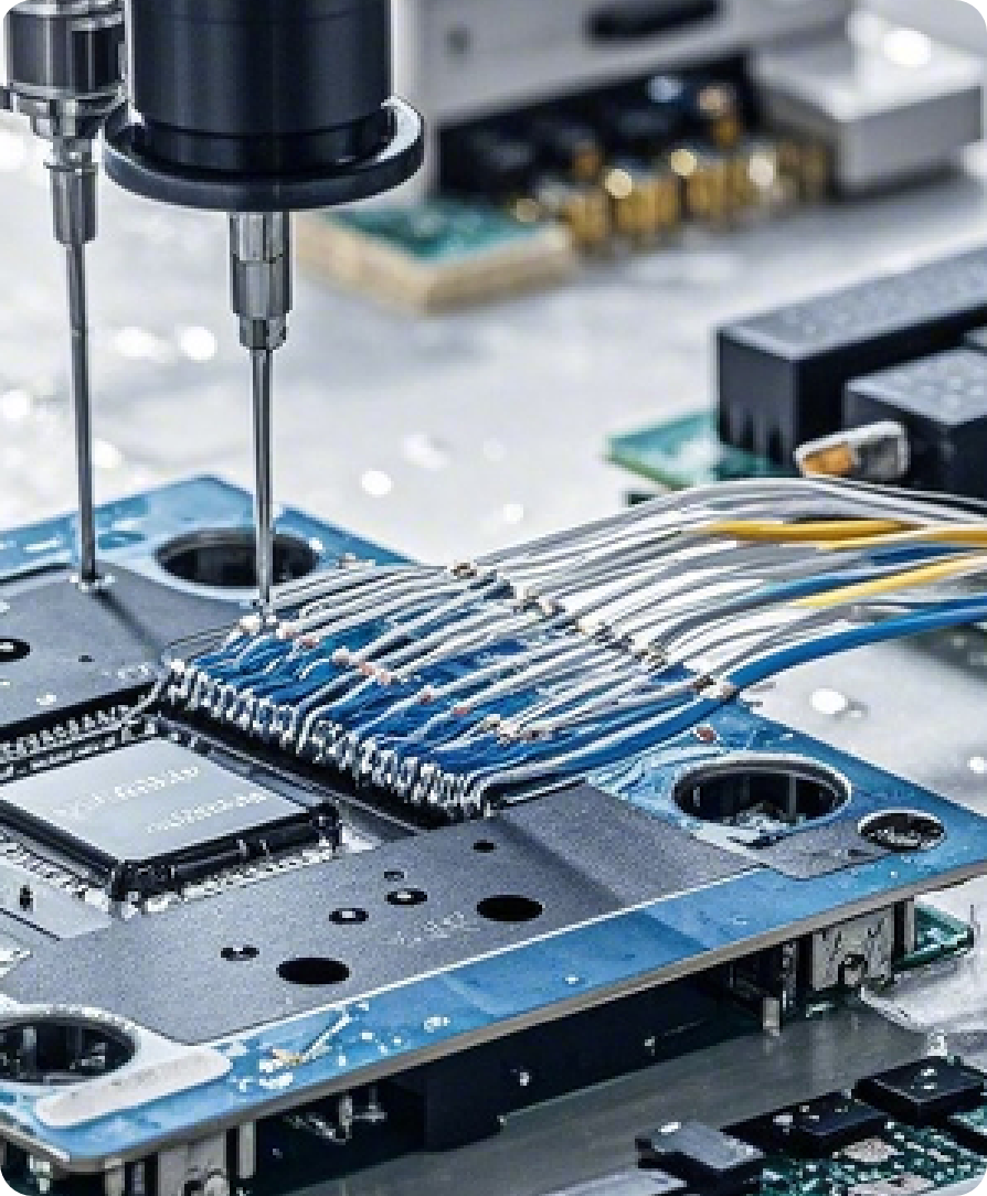
- Организация производственного процесса: Полностью автоматизированное сверление на станках с ЧПУ и высокоточное нанесение медного покрытия.
- Поддержка технологических процессов: односторонние/двусторонние, многослойные, гибкие печатные платы и платы с высокой плотностью межсоединений (HDI).
- Строгий экологический контроль: регулирование температуры и тщательная очистка предотвращают загрязнение и обеспечивают ровные, гладкие поверхности.
Шаг 4
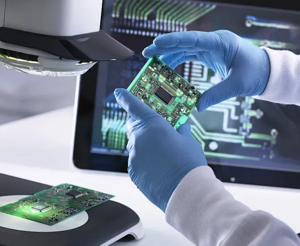
Контроль качества
- 100% автоматическая оптическая инспекция (AOI): мгновенно обнаруживает обрывы, короткие замыкания и отсутствующие контактные площадки.
- Внутрисхемное тестирование (ICT): проверяет контрольные точки на печатной плате для обеспечения полной целостности сигнала.
- Рентгеновский послойный контроль: позволяет проверить скрытые/глухие переходные отверстия и качество ламинирования.
Шаг 5
Доставка и поддержка
- Антистатическая вакуумная упаковка с осушителем.
- Доставка осуществляется несколькими курьерскими службами: EMS, DHL, UPS, все отправления полностью отслеживаются.
- Номер для отслеживания отправления предоставляется в течение 24 часов после отправки, а также предоставляется круглосуточная техническая поддержка 7 дней в неделю (12 часов в сутки).

Возможности
| Возможности | Параметры | Подробности |
|---|---|---|
| Слои | До 50 слоев | Прототипирование печатных плат с высокой плотностью монтажа (HDI) до 50 слоев, идеально подходит для телекоммуникационной, аэрокосмической и оборонной отраслей. |
| Максимальный размер | 600 × 500 мм | Максимальный размер панели 600 × 500 мм, поддерживает крупноформатные промышленные системы управления, светодиодные дисплеи и автомобильную электронику. |
| Толщина | 0,2 – 7,0 мм | Толщина платы: от 0,2 мм до 7,0 мм, от ультратонких гибких (для носимых устройств) до жестких алюминиевых подложек (высокая жесткость). |
| Толщина меди | 0,33 – 12 унций | Вес меди 0,33–12 унций, от стандартных до сильноточных силовых плат с улучшенным отводом тепла. |
| Минимальная ширина/расстояние между линиями | 2,5 мил / 2,5 мил | Минимальная ширина/расстояние между линиями 2,5 мил, поддерживает шаг выводов микросхем 0,5 мм и меньше для поверхностного монтажа высокой плотности. |
| Минимальный диаметр сверления отверстий | 6 мил | Минимальный диаметр сверления 6 мил позволяет создавать микроскопические глухие/скрытые переходные отверстия для прецизионных ВЧ и СВЧ соединений. |
| Зазор между отверстием и проводником | 5 мил | Минимальная ширина кольцевого пояска 5 мил, соответствует стандартам IPC-2221 для уменьшения помех между проводником и отверстием. |
| Допуск по импедансу | ±10% или ±5% | Контролируемый импеданс ±5% (±10% опционально), подходит для высокоскоростных сигналов (USB3.0, PCIe, RF) и стандартных цифровых схем |
| Допуск на размеры | ±0,1 мм | Допуск на контур ±0,1 мм обеспечивает механическую точность для плотной сборки промышленных и бытовых изделий. |
| Материалы | Shengyi S1000 2, S1141, ITEQ IT180A, на основе алюминия и меди, серия Rogers RF (4350B, 4003C, 3003), серия RT/VT, DuPont PI, серия ISOLA FR, Megtron 4/6 | Варианты материалов: FR-4, алюминий, медь, высокочастотные материалы (Rogers, Megtron) и гибкий полиимид. |
| Размер отверстия в защитном покрытии: | ≥ 0,6 мм × 0,6 мм | Минимальный размер окна в гибком защитном покрытии 0,6 × 0,6 мм гарантирует надежную прочность сцепления и ламинирования для носимых устройств и медицинских датчиков, подвергающихся интенсивным изгибам. |
| Обработка поверхности | ENIG, ENEPIG, I Ag, OSP, HAL (без свинца), тонкое золотое покрытие, твердое золотое покрытие |
Примеры использования в промышленности

Прототипные платы для аэрокосмической и оборонной промышленности
- Области применения: аэрокосмическая и оборонная промышленность (требования к высокой надежности), многослойные конструкции с высокой плотностью монтажа, строгий контроль импеданса.
- Характеристики: Соответствие стандарту IPC-6012 Class 3, допуск по импедансу ±5%, покрытие ENIG.

Прототипы медицинских устройств
- Области применения: Миниатюрные схемы высокой плотности для медицинских устройств, требующие использования биосовместимых материалов и сверхтонких печатных плат.
- Особенности: минимальная ширина линии 2,5 мил, гибкая подложка из полиимида, 100% автоматический оптический контроль и внутрисхемное тестирование.

Прототипирование автомобильной электроники
- Области применения: Миниатюрные схемы высокой плотности для медицинских устройств, требующие использования биосовместимых материалов и сверхтонких печатных плат.
- Features: 2.5 mil minimum line width, PI flex substrate, 100% AOI + ICT inspection.

Интернет вещей и бытовая электроника
- Области применения: Быстрая разработка и тестирование систем «умного дома», носимых устройств и бытовой электроники.
- Особенности: Поддержка сверхтонких печатных плат толщиной 0,2 мм, интеграция гибких и жестких элементов, а также комплексное выполнение всех этапов производства.

Часто задаваемые вопросы
The manufacturing time of PCB prototypes varies due to various factors, including the complexity of the circuit board, the manufacturing plant’s production capacity, and order volume.
Generally speaking, simple single or double-sided board prototypes can be manufactured in a few days, while complex multi-layer boards or circuit boards containing special processes such as blind holes and buried holes may require longer time.
To shorten the manufacturing cycle, it is recommended to choose PCB manufacturers with advanced manufacturing equipment and efficient production processes.
Poor circuit: such as open circuit, short circuit, circuit width or spacing not meeting design requirements, etc.
Pad issues: Pad detachment, incorrect pad size, mismatch between pad and component pins, etc.
Drilling problems: aperture deviation, incorrect hole position, poor hole wall quality, etc.
Surface treatment defects: such as uneven coating of solder mask, blurry character printing, insufficient coating thickness, etc.
These issues may be caused by design errors, improper process control during manufacturing, or material quality problems.
Therefore, a detailed design review should be conducted before manufacturing, reliable manufacturers should be selected, and strict quality control should be implemented during the manufacturing process.
Manufacturing capability: Does the manufacturer have advanced manufacturing equipment and processes to meet your design requirements and production capacity needs.
Quality control: Whether the manufacturer has established a sound quality management system and can provide reliable quality assurance and after-sales service.
Price and delivery time: Compare the prices and delivery times of different manufacturers and choose the manufacturer with high cost-effectiveness.
Technical support: Does the manufacturer provide technical support and solutions, and can they assist in solving problems during the design or manufacturing process.
Electrical performance: The dielectric constant, dielectric loss, resistivity, and other electrical properties of the material should meet the design requirements.
Mechanical strength: The mechanical properties such as bending strength and impact strength of the material should be sufficient to ensure the reliability and durability of the circuit board.
Thermal stability: The material should have good thermal stability and be able to withstand certain temperature changes without deformation or cracking.
Processing performance: The material should be easy to process, such as drilling, etching, electroplating, and other processes should be able to proceed smoothly.
Cost: While ensuring performance, the cost of materials should be considered and materials with high cost-effectiveness should be selected.
Electrical testing: Check the conductivity, insulation resistance, withstand voltage and other electrical performance of the circuit.
Functional testing: Verify whether the circuit board works according to design requirements, including signal transmission, power distribution, and other functions.
Reliability testing: such as thermal cycling testing, wet heat testing, vibration testing, etc., to evaluate the reliability of circuit boards during long-term use.
Appearance inspection: Check the appearance quality of the circuit board, such as solder joint quality, solder mask coating, character printing clarity, etc