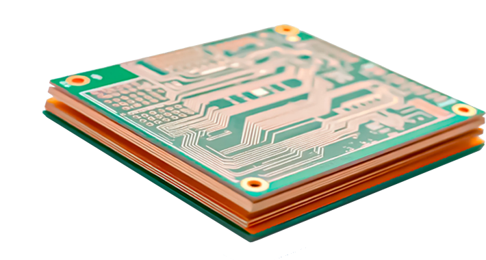
יצרן אב טיפוס של PCB
שירותי ייצור אב טיפוס מהיר וייצור PCB גמיש בנפח
כספק מוביל בסין של מעגלים מודפסים גמישים, אנו מתמחים בייצור מעגלים גמישים באיכות גבוהה – החל מאב טיפוס מהיר ועד לייצור מעגלים מודפסים גמישים בנפח מלא. העלו את קבצי Gerber שלכם עכשיו לקבלת הצעת מחיר מהירה ואמינה.


מהו אב טיפוס של PCB?
אבות טיפוס של PCB כרוך בייצור מהיר של אצווה קטנה של לוחות מקבצי תכנון לפני ייצור המוני לצורך אימות פונקציונלי, בדיקות ביצועים והערכת תהליכים. אבות טיפוס אלה מאפשרים למהנדסים לאתר במהירות פגמי תכנון ולמטב פריסות, ובכך להבטיח ייצור בקנה מידה גדול ללא רבב.
למה לבחור בשירות ייצור אבות טיפוס של PCB שלנו?
Standard lead time of 5–7 business days; 3‑day expedited delivery for urgent R&D needs.
Minimum line width/spacing of 4 mil; hole sizes down to 0.2 mm; supports multilayer, flex, and HDI boards.
IPC-610 compliant with AOI, ICT, and X-ray inspections—100% coverage to eliminate manufacturing defects.
From prototyping and SMT assembly to stencil fabrication and DFM checks, streamlining communication and shortening project cycles.
תהליך וזרימת עבודה
שלב 1
הגשת עיצוב
- העלה קבצי גרבר/CAD
- תומך בפורמטים Gerber 274X, ODB++ ו-IPC-2581
- קבצים מאוחסנים אוטומטית בארכיון עם מזהה פרויקט ייחודי
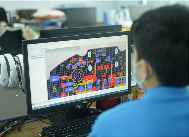
שלב 2
סקירה טכנית
- הערכה ידנית תוך שעתיים
- בדיקות עיקריות: רוחב/מרווח מינימלי בין הקווים, קוטר החור, פתחי מסיכת הלחמה ומרווח מסיכה
- הצעות אופטימיזציה הונפקו ואושרו באמצעות דוא"ל או טלפון
שלב 3
אב טיפוס וייצור
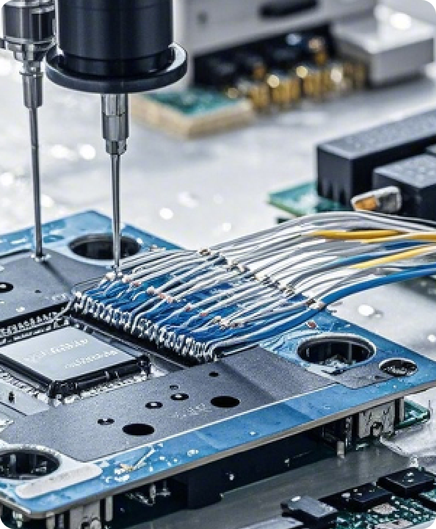
- הקמת רצפת הייצור: קידוח CNC אוטומטי לחלוטין ולמינציה של נחושת בדיוק גבוה.
- תמיכה בתהליך: לוחות חד-צדדיים/דו-צדדיים, רב-שכבתיים, גמישים ו-HDI
- בקרת סביבה קפדנית: ויסות טמפרטורה וניקוי יסודי מונעים זיהום ומבטיחים משטחים שטוחים ואחידים
שלב 4
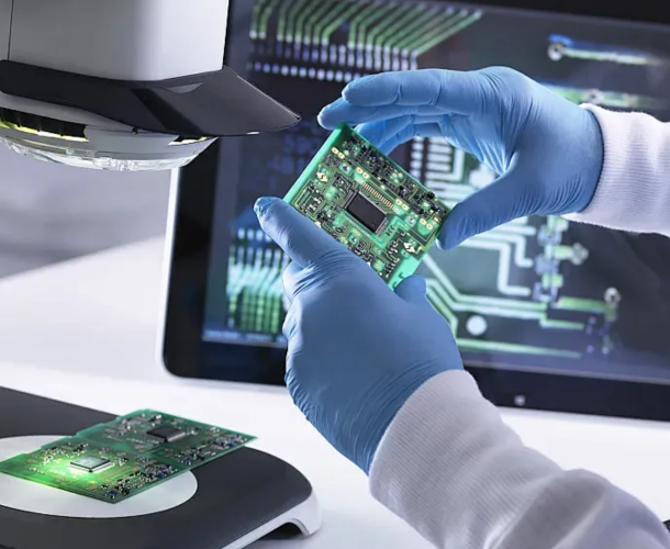
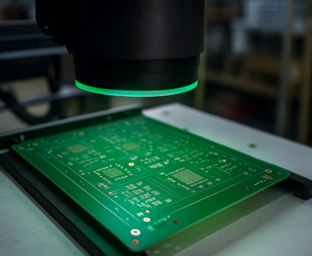
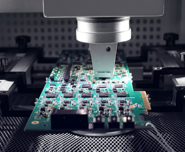
בדיקת איכות
- בדיקה אופטית אוטומטית של 100% AOI: מזהה באופן מיידי פתחים, קצרים ורפידות חסרות
- בדיקות ICT בתוך המעגל: מכסה נקודות בדיקה ברשת כדי להבטיח שלמות אות מלאה
- בדיקת שכבות רנטגן: מאמתת ויאסים קבורים/עיוורים ואיכות למינציה
שלב 5
משלוח ותמיכה
- אריזת ואקום אנטי-סטטית עם חומר יבוש
- מספר ספקים: EMS, DHL, UPS, כולם ניתנים למעקב מלא
- מספר מעקב נשלח תוך 24 שעות ממועד המשלוח ותמיכה טכנית מקוונת 7×12 שעות

יכולות
| יכולת | פרמטרים | פרטים |
|---|---|---|
| שכבות | עד 50 שכבות | אב טיפוס HDI של עד 50 שכבות, אידיאלי עבור יישומי טלקום, תעופה וחלל וביטחון |
| גודל מקסימלי | 600 × 500 מ"מ | גודל פאנל מקסימלי 600 × 500 מ"מ, תומך בבקרה תעשייתית בפורמט גדול, צגי LED ואלקטרוניקה לרכב |
| עובי | 0.2 – 7.0 מ"מ | עובי לוח 0.2 מ"מ–7.0 מ"מ, החל ממצעי אלומיניום דקים במיוחד וגמישים (לבישים) ועד מצעי אלומיניום קשיחים (בעלי קשיחות גבוהה). |
| עובי נחושת | 0.33 – 12 אונקיות | משקל נחושת 0.33 אונקיות–12 אונקיות, מלוחות חשמל סטנדרטיים ועד לוחות חשמל בעלי זרם גבוה עם פיזור חום משופר |
| רוחב/מרווח מינימלי בין קו | 2.5 מיל / 2.5 מיל | מרווח/מרווח מינימלי בין קו 2.5 מיל, תומך במרווחי שבבים של 0.5 מ"מ ומעלה עבור SMT בצפיפות גבוהה |
| חור קידוח מינימלי | 6 מיל | קידוח מינימלי 6 מיל, מאפשר ויאים מיקרו-עיוורים/קבורים עבור חיבורי RF ומיקרוגל מדויקים |
| מרווח חור-לקו | 5 מיל | טבעת טבעתית מינימלית 5 מיל, עומדת בתקני IPC-2221 להפחתת הפרעות מסלול-לחור |
| סבילות עכבה | ±10% או ±5% | עכבה מבוקרת ±5% (±10% אופציונלי), מתאימה לאותות במהירות גבוהה (USB3.0, PCIe, RF) ולמעגלים דיגיטליים סטנדרטיים |
| סבילות מידות | ±0.1 מ"מ | סבילות קו מתאר ±0.1 מ"מ, מבטיחה דיוק מכני עבור מכלולים תעשייתיים וצרכניים בעלי התאמה הדוקה |
| חומר | Shengyi S1000 2, S1141, ITEQ IT180A, מבוסס אלומיניום ונחושת, סדרת Rogers RF (4350B, 4003C, 3003), סדרת RT/VT, DuPont PI, סדרת ISOLA FR, Megtron 4/6 Wait | אפשרויות חומרים, FR-4, אלומיניום, נחושת, תדר גבוה (Rogers, Megtron), ו-PI גמיש |
| גודל פתח כיסוי | ≥ 0.6 מ"מ × 0.6 מ"מ | חלון כיסוי גמיש מינימום 0.6 × 0.6 מ"מ, מבטיח חוזק קילוף אמין ולמינציה עבור מכשירים לבישים בעלי כיפוף רב וחיישנים רפואיים |
| טיפול פני שטח | ENIG, ENEPIG, I Ag, OSP, HAL (ללא עופרת), זהב פלאש, זהב קשה |
מקרי שימוש בתעשייה

לוחות אב טיפוס לתעופה וחלל והגנה
- יישומים: אמינות ברמת תעופה וחלל, תכנוני HDI רב-שכבתיים ובקרת עכבה קפדנית.
- מאפיינים: IPC-6012 Class3, סובלנות עכבה של ±5%, גימור ENIG.

אבות טיפוס של מכשור רפואי
- יישומים: מעגלים מיניאטוריים בצפיפות גבוהה עבור מכשירים רפואיים הדורשים חומרים ביו-תואמים ולוחות דקים במיוחד.
- מאפיינים: רוחב קו מינימלי של 2.5 מיל, מצע גמיש PI, 100% AOI + בדיקת ICT.

אב טיפוס של אלקטרוניקה לרכב
- יישומים: מעגלים מיניאטוריים בצפיפות גבוהה עבור מכשירים רפואיים הדורשים חומרים ביו-תואמים ולוחות דקים במיוחד.
- מאפיינים: רוחב קו מינימלי של 2.5 מיל, מצע גמיש PI, 100% AOI + בדיקת ICT.

האינטרנט של הדברים ואלקטרוניקה צרכנית
- יישומים: איטרציה מהירה של מערכות בית חכם, מכשירים לבישים ואלקטרוניקה צרכנית.
- מאפיינים: תמיכה בלוחות מודפסים דקים במיוחד בעובי 0.2 מ"מ, אינטגרציה גמישה-קשיחה ואספקה מרובת תהליכים במקום אחד.

שאלות נפוצות
The manufacturing time of PCB prototypes varies due to various factors, including the complexity of the circuit board, the manufacturing plant’s production capacity, and order volume.
Generally speaking, simple single or double-sided board prototypes can be manufactured in a few days, while complex multi-layer boards or circuit boards containing special processes such as blind holes and buried holes may require longer time.
To shorten the manufacturing cycle, it is recommended to choose PCB manufacturers with advanced manufacturing equipment and efficient production processes.
Poor circuit: such as open circuit, short circuit, circuit width or spacing not meeting design requirements, etc.
Pad issues: Pad detachment, incorrect pad size, mismatch between pad and component pins, etc.
Drilling problems: aperture deviation, incorrect hole position, poor hole wall quality, etc.
Surface treatment defects: such as uneven coating of solder mask, blurry character printing, insufficient coating thickness, etc.
These issues may be caused by design errors, improper process control during manufacturing, or material quality problems.
Therefore, a detailed design review should be conducted before manufacturing, reliable manufacturers should be selected, and strict quality control should be implemented during the manufacturing process.
Manufacturing capability: Does the manufacturer have advanced manufacturing equipment and processes to meet your design requirements and production capacity needs.
Quality control: Whether the manufacturer has established a sound quality management system and can provide reliable quality assurance and after-sales service.
Price and delivery time: Compare the prices and delivery times of different manufacturers and choose the manufacturer with high cost-effectiveness.
Technical support: Does the manufacturer provide technical support and solutions, and can they assist in solving problems during the design or manufacturing process.
Electrical performance: The dielectric constant, dielectric loss, resistivity, and other electrical properties of the material should meet the design requirements.
Mechanical strength: The mechanical properties such as bending strength and impact strength of the material should be sufficient to ensure the reliability and durability of the circuit board.
Thermal stability: The material should have good thermal stability and be able to withstand certain temperature changes without deformation or cracking.
Processing performance: The material should be easy to process, such as drilling, etching, electroplating, and other processes should be able to proceed smoothly.
Cost: While ensuring performance, the cost of materials should be considered and materials with high cost-effectiveness should be selected.
Electrical testing: Check the conductivity, insulation resistance, withstand voltage and other electrical performance of the circuit.
Functional testing: Verify whether the circuit board works according to design requirements, including signal transmission, power distribution, and other functions.
Reliability testing: such as thermal cycling testing, wet heat testing, vibration testing, etc., to evaluate the reliability of circuit boards during long-term use.
Appearance inspection: Check the appearance quality of the circuit board, such as solder joint quality, solder mask coating, character printing clarity, etc