Hersteller von Prototypen-Leiterplatten
Hersteller von Prototypen-Leiterplatten
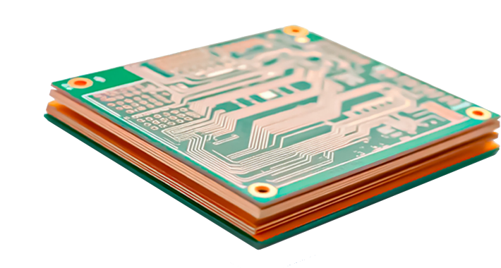
Als führender chinesischer Anbieter von flexiblen Leiterplatten sind wir auf die Herstellung hochwertiger flexibler Schaltungen spezialisiert – vom schnellen Prototyping bis zur Serienfertigung flexibler Leiterplatten. Laden Sie jetzt Ihre Gerber-Dateien hoch und erhalten Sie ein schnelles und zuverlässiges Angebot.


Was ist PCB-Prototyping?
Beim Leiterplatten-Prototyping wird vor der Massenproduktion schnell eine kleine Serie von Leiterplatten anhand der Designdateien hergestellt, um die Funktionalität zu überprüfen, Leistungstests durchzuführen und den Produktionsprozess zu evaluieren. Diese Prototypen ermöglichen es Ingenieuren, Konstruktionsfehler schnell zu erkennen und Layouts zu optimieren, um eine fehlerfreie Serienfertigung zu gewährleisten.
Warum sollten Sie sich für unseren Prototypenfertigungsservice für Leiterplatten entscheiden?
Standard lead time of 5–7 business days; 3‑day expedited delivery for urgent R&D needs.
Minimum line width/spacing of 4 mil; hole sizes down to 0.2 mm; supports multilayer, flex, and HDI boards.
IPC-610 compliant with AOI, ICT, and X-ray inspections—100% coverage to eliminate manufacturing defects.
From prototyping and SMT assembly to stencil fabrication and DFM checks, streamlining communication and shortening project cycles.
Prozess und Arbeitsablauf
Schritt 1
Design-Einreichung
- Gerber-/CAD-Dateien hochladen
- Unterstützt die Formate Gerber 274X, ODB++ und IPC-2581.
- Dateien werden automatisch mit einer eindeutigen Projekt-ID archiviert.
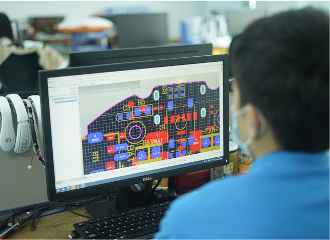
Schritt 2
Technische Überprüfung
- Manuelle Bewertung innerhalb von 2 Stunden
- Wichtige Prüfungen: minimale Leiterbahnbreite/Abstand, Lochdurchmesser, Lötstopplacköffnungen und Lötstopplackabstand.
- Optimierungsvorschläge werden per E-Mail oder Telefon übermittelt und bestätigt.
Schritt 3
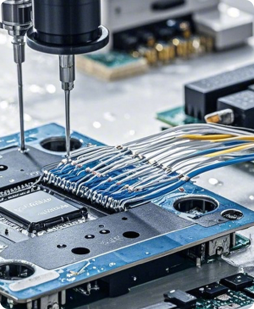
Prototypenentwicklung und Fertigung
- Fertigungsanlagen: Vollautomatische CNC-Bohrmaschinen und hochpräzise Kupferkaschierung.
- Prozessunterstützung: Einseitige/doppelseitige, mehrlagige, flexible und HDI-Leiterplatten
- Strenge Umweltkontrollen: Temperaturregulierung und gründliche Reinigung verhindern Verunreinigungen und gewährleisten ebene, gleichmäßige Oberflächen.
Schritt 4
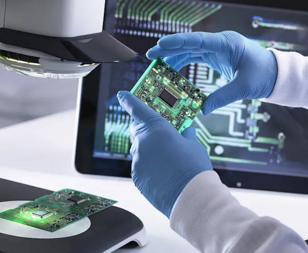
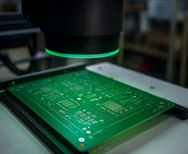
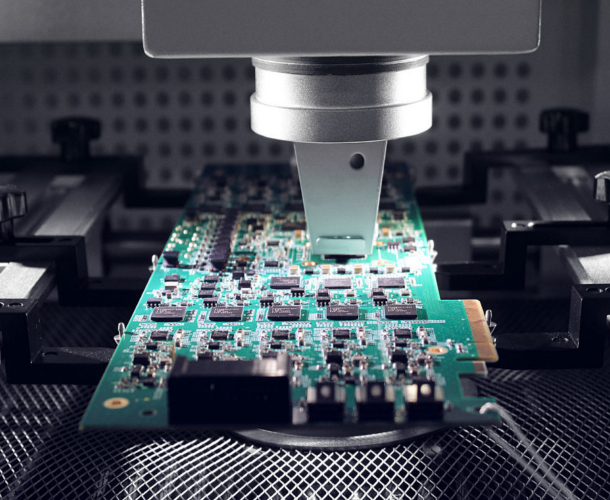
Qualitätsinspektion
- 100% AOI Automatische optische Inspektion: erkennt sofort Unterbrechungen, Kurzschlüsse und fehlende Lötstellen.
- ICT-In-Circuit-Test: Überprüft die Testpunkte auf der Leiterplatte, um eine vollständige Signalintegrität zu gewährleisten.
- Röntgen-Schichtinspektion: Überprüfung von vergrabenen/verdeckten Durchkontaktierungen und der Laminierungsqualität.
Schritt 5
Versand & Support
- Antistatische Vakuumverpackung mit Trockenmittel
- Mehrere Versanddienstleister: EMS, DHL, UPS, alle mit Sendungsverfolgung.
- Die Sendungsverfolgungsnummer wird innerhalb von 24 Stunden nach dem Versand verschickt, und es steht Ihnen ein technischer Online-Support rund um die Uhr (7 Tage die Woche, 12 Stunden am Tag) zur Verfügung.

Fähigkeiten
| Fähigkeit | Parameter | Details |
|---|---|---|
| Lagen | Bis zu 50 Lagen | Prototypenfertigung mit bis zu 50 Lagen (HDI), ideal für Anwendungen in den Bereichen Telekommunikation, Luft- und Raumfahrt und Verteidigung. |
| Maximale Größe | 600 × 500 mm | Maximale Platinengröße: 600 × 500 mm, geeignet für großformatige Industriesteuerungen, LED-Displays und Automobilelektronik. |
| Dicke | 0,2 – 7,0 mm | Leiterplattendicke: 0,2 mm–7,0 mm, von ultradünnen, flexiblen (Wearables) bis hin zu starren Aluminiumsubstraten (hohe Steifigkeit). |
| Kupferstärke | 0,33 – 12 oz | Kupfergewicht: 0,33 oz – 12 oz, von Standard- bis hin zu Hochleistungs-Leiterplatten mit verbesserter Wärmeableitung |
| Minimale Leiterbahnbreite / Leiterbahnabstand | 2,5 mil / 2,5 mil | Minimale Leiterbahnbreite/Leiterbahnabstand 2,5 mil, unterstützt Chip-Gehäuse-Raster von 0,5 mm und feinere Rastermaße für hochdichte SMT-Bestückung. |
| Mindestbohrlochdurchmesser | 6 mil | Mindestbohrlochdurchmesser 6 mil, ermöglicht mikrofeine Sackloch-/Durchkontaktierungen für präzise HF- und Mikrowellenverbindungen |
| Abstand zwischen Bohrung und Leiterbahn | 5 mil | Mindestbreite des Ringwulstes: 5 mil, entspricht den IPC-2221-Standards zur Reduzierung von Interferenzen zwischen Leiterbahn und Bohrung |
| Impedanztoleranz | ±10 % oder ±5 % | Kontrollierte Impedanz ±5 % (±10 % optional), geeignet für Hochgeschwindigkeitssignale (USB 3.0, PCIe, HF) und Standard-Digitalschaltungen |
| Maßtoleranz | ±0,1 mm | Konturtoleranz ±0,1 mm gewährleistet mechanische Präzision für passgenaue Baugruppen in Industrie und Konsumgüterbereich. |
| Material | Shengyi S1000-2, S1141, ITEQ IT180A, Aluminiumbasis & Kupferbasis, Rogers RF-Serie (4350B, 4003C, 3003), RT/VT-Serie, DuPont PI, ISOLA FR-Serie, Megtron 4/6 | Materialoptionen: FR-4, Aluminium, Kupfer, Hochfrequenzmaterialien (Rogers, Megtron) und flexibles PI |
| Abmessungen der Abdeckfolienöffnung | ≥ 0,6 mm × 0,6 mm | Das flexible Abdeckfolienfenster mit einer Mindestgröße von 0,6 × 0,6 mm gewährleistet zuverlässige Haftfestigkeit und Laminierung für biegebeanspruchte Wearables und medizinische Sensoren. |
| Oberflächenbehandlung | ENIG, ENEPIG, I Ag, OSP, HAL (bleifrei), Flash-Gold, Hartgold |
Anwendungsfälle in der Industrie

Prototypenplatinen für Luft- und Raumfahrt und Verteidigung
- Anwendungsbereiche: Zuverlässigkeit nach Luft- und Raumfahrt- und Militärstandards, mehrschichtige HDI-Designs und strenge Impedanzkontrolle.
- Eigenschaften: IPC-6012 Klasse 3, Impedanztoleranz ±5 %, ENIG-Oberflächenveredelung.

Prototypen medizinischer Geräte
- Anwendungsbereiche: Miniaturisierte, hochintegrierte Schaltungen für medizinische Geräte, die biokompatible Materialien und ultradünne Leiterplatten erfordern.
- Merkmale: Mindestlinienbreite von 2,5 mil, PI-Flexsubstrat, 100% AOI- und ICT-Inspektion.

Prototypenentwicklung für Automobilelektronik
- Anwendungsbereiche: Miniaturisierte, hochintegrierte Schaltungen für medizinische Geräte, die biokompatible Materialien und ultradünne Leiterplatten erfordern.
- Merkmale: Mindestlinienbreite von 2,5 mil, PI-Flexsubstrat, 100% AOI- und ICT-Inspektion.

IoT und Unterhaltungselektronik
- Anwendungsbereiche: Schnelle Entwicklung von Smart-Home-Systemen, tragbaren Geräten und Unterhaltungselektronik.
- Merkmale: Unterstützt ultradünne 0,2 mm Leiterplatten, flexible-starre Integration und bietet eine Komplettlösung mit mehreren Fertigungsprozessen.

Häufig gestellte Fragen
The manufacturing time of PCB prototypes varies due to various factors, including the complexity of the circuit board, the manufacturing plant’s production capacity, and order volume.
Generally speaking, simple single or double-sided board prototypes can be manufactured in a few days, while complex multi-layer boards or circuit boards containing special processes such as blind holes and buried holes may require longer time.
To shorten the manufacturing cycle, it is recommended to choose PCB manufacturers with advanced manufacturing equipment and efficient production processes.
Poor circuit: such as open circuit, short circuit, circuit width or spacing not meeting design requirements, etc.
Pad issues: Pad detachment, incorrect pad size, mismatch between pad and component pins, etc.
Drilling problems: aperture deviation, incorrect hole position, poor hole wall quality, etc.
Surface treatment defects: such as uneven coating of solder mask, blurry character printing, insufficient coating thickness, etc.
These issues may be caused by design errors, improper process control during manufacturing, or material quality problems.
Therefore, a detailed design review should be conducted before manufacturing, reliable manufacturers should be selected, and strict quality control should be implemented during the manufacturing process.
Manufacturing capability: Does the manufacturer have advanced manufacturing equipment and processes to meet your design requirements and production capacity needs.
Quality control: Whether the manufacturer has established a sound quality management system and can provide reliable quality assurance and after-sales service.
Price and delivery time: Compare the prices and delivery times of different manufacturers and choose the manufacturer with high cost-effectiveness.
Technical support: Does the manufacturer provide technical support and solutions, and can they assist in solving problems during the design or manufacturing process.
Electrical performance: The dielectric constant, dielectric loss, resistivity, and other electrical properties of the material should meet the design requirements.
Mechanical strength: The mechanical properties such as bending strength and impact strength of the material should be sufficient to ensure the reliability and durability of the circuit board.
Thermal stability: The material should have good thermal stability and be able to withstand certain temperature changes without deformation or cracking.
Processing performance: The material should be easy to process, such as drilling, etching, electroplating, and other processes should be able to proceed smoothly.
Cost: While ensuring performance, the cost of materials should be considered and materials with high cost-effectiveness should be selected.
Electrical testing: Check the conductivity, insulation resistance, withstand voltage and other electrical performance of the circuit.
Functional testing: Verify whether the circuit board works according to design requirements, including signal transmission, power distribution, and other functions.
Reliability testing: such as thermal cycling testing, wet heat testing, vibration testing, etc., to evaluate the reliability of circuit boards during long-term use.
Appearance inspection: Check the appearance quality of the circuit board, such as solder joint quality, solder mask coating, character printing clarity, etc