Grundlagen: Wellenlöten und selektives Löten erklärt
Die Through-Hole-Technologie (THT) stützt sich weiterhin stark auf Massenlötverfahren. Unter ihnen dominieren selektives Löten und Wellenlöten. Beide erzeugen zuverlässige THT-Lötstellen, unterscheiden sich jedoch deutlich in Wirkprinzip, Prozessfenster und Einsatzgrenzen.
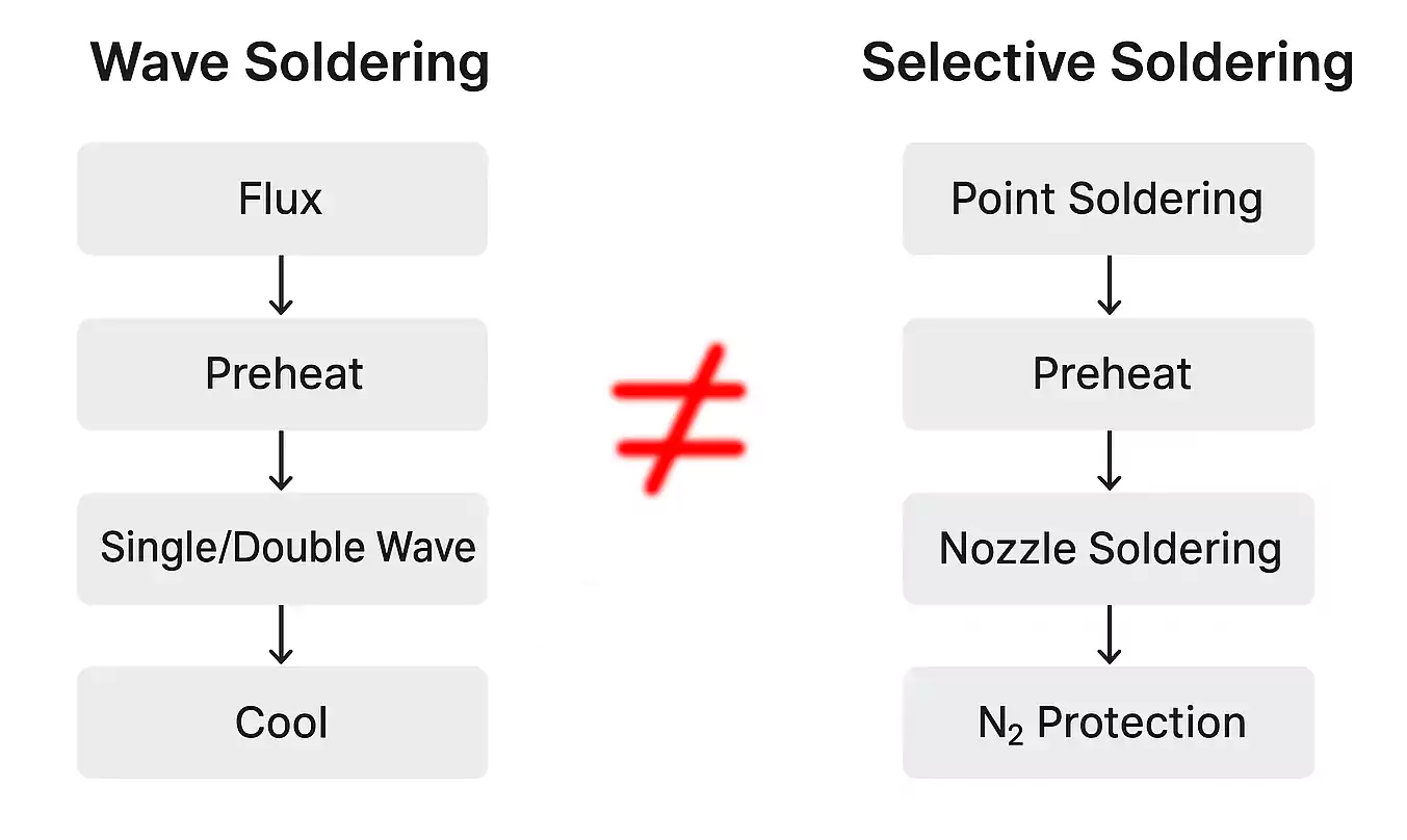
1) Wellenlöten (Ganzplatinen-Prozess)
Beim Wellenlöten wird die gesamte Unterseite der Leiterplatte in eine „Lötwelle“ aus geschmolzenem Lot getaucht. Es ist ein hochproduktiver Ganzplatinen-Prozess, besonders geeignet für Baugruppen mit vielen THT-Pins.
Prozessablauf:
- Flussmittelauftrag – Schaum- oder Sprühflussmittel beschichtet die Unterseite gleichmäßig, entfernt Oxide und fördert die Benetzung.
- Vorheizen – Kontrollierte Erwärmung treibt Lösungsmittel aus, aktiviert die Chemie und reduziert thermischen Schock.
- Kontakt mit der Lötwelle – Die Platine läuft über eine einfache oder doppelte Lötwelle:
- Laminare Welle sorgt für gleichmäßige Benetzung großer Bereiche.
- Turbulente Welle verbessert die Durchkontaktierungsfüllung und mindert Abschattung.
- Abkühlen und Erstarren – Die Lötstellen erstarren beim Austritt aus der Welle.
Wesentliche Punkte:
- Parameterfenster (typisch): Vorheizen 90–130 °C; Löttemperatur im Tiegel 245–265 °C; Förderbandgeschwindigkeit 1–2 m/min.
- Designeinfluss: Abschattung kann hinter hohen Bauteilen zu Nichtbenetzung führen; Robber-Pads und Thieving-Features werden oft hinzugefügt, um den Lotfluss zu lenken.
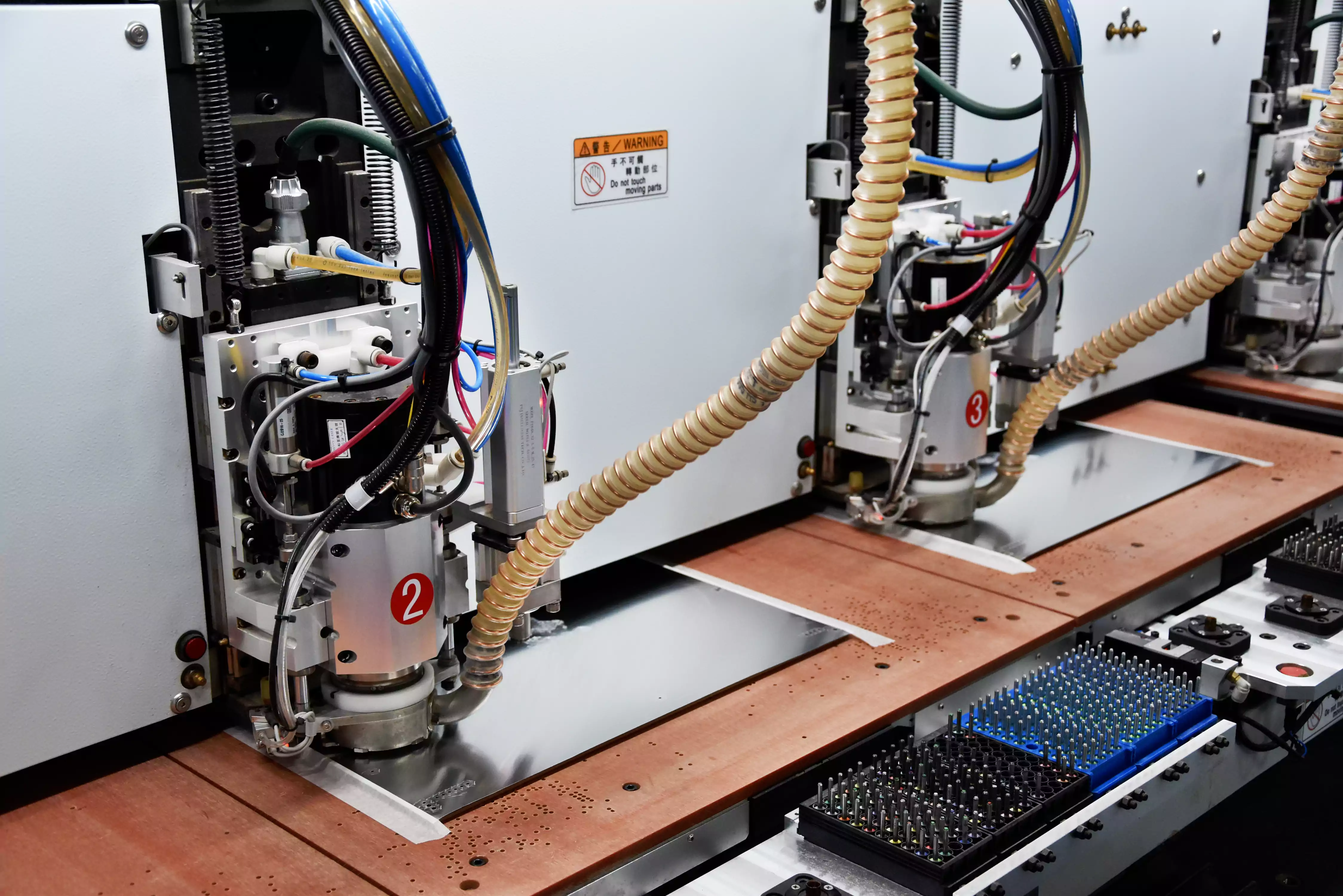
2) Selektives Löten (Lokalprozess)
Selektives Löten adressiert die Grenzen des Wellenlötens bei Mischbestückungen. Statt die gesamte Platine zu exponieren, werden nur definierte THT-Lötstellen bearbeitet – ideal für Baugruppen mit zusätzlichen SMT-Komponenten.
Prozessablauf:
- Flussmitteldeposition – Mini-Sprüh- oder Drop-Jet-Auftrag gezielt auf ausgewählte Pads.
- Lokalisiertes Vorheizen – Erwärmt nur den geflussten Bereich zur Aktivierung und besseren Benetzung.
- Mini-Welle – Eine programmierte Düse oder Fontäne bildet eine lokale Lötwelle, die die Lötstelle kontaktiert:
- Mini-Sprühdüsen erlauben enge Abstände.
- Fontänendüsen eignen sich für größere Steckverbinder.
- Stickstoffatmosphäre – Schirmt die Lötoberfläche vor Oxidation ab, ermöglicht stabile Benetzung und weniger Brücken.
Wesentliche Punkte:
- Programmierspur: Düsenbahn, Verweilzeit und Abhebegeschwindigkeit werden pro Bauteil optimiert.
- Prozesskontrolle: Engeres thermisches Profil als beim Wellenlöten, geringere Belastung hitzesensibler Teile.
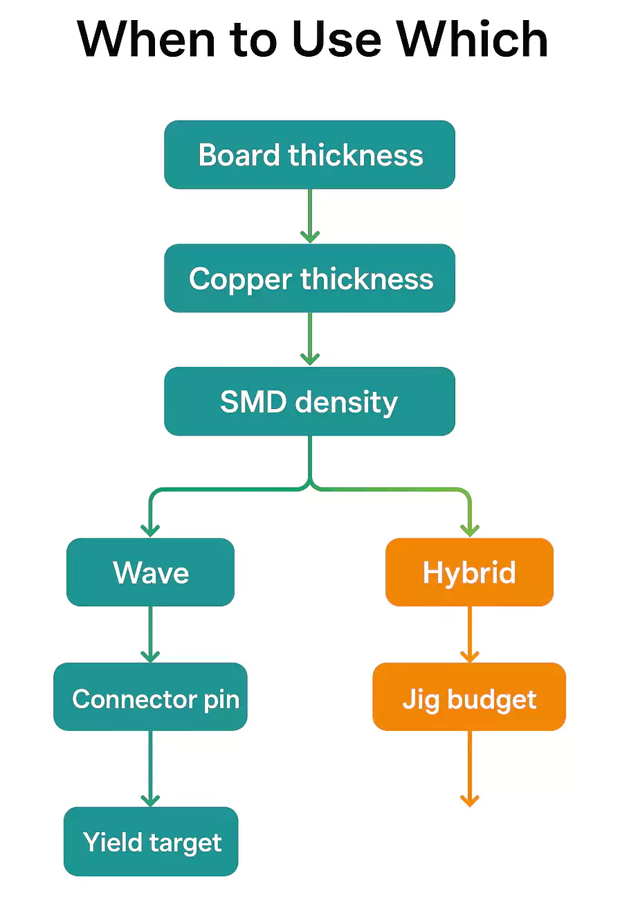
Wann welche Methode? Anwendungsfälle und Grenzen
1) Nach Stückliste (BOM)
- Welle: Effizient bei hohem THT-Anteil, großen Steckverbindern oder vielen wiederkehrenden Pins.
- Selektiv: Besser, wenn THT-Teile spärlich und mit dichten SMT-Bereichen gemischt sind oder starke Höhenunterschiede/temperaturempfindliche Bauteile vorliegen.
2) Nach PCB-Design
- Welle: Schwieriger bei doppelseitiger Bestückung, engem Bauteilabstand oder uneinheitlichen Orientierungen (Risiko Abschattung/Brücken).
- Selektiv: Programmierbare Düsen und lokale Erwärmung handhaben diese Randbedingungen zuverlässiger. Korrekte Lötstopplack-Öffnungen und Thieving-Pads bleiben in beiden Fällen wichtig.
3) Nach Fertigungsstrategie
- Welle: Niedrigste Stückkosten bei hohen, stabilen Volumina – vorausgesetzt, Vorlaufzeit/Kosten für Vorrichtungen sind vertretbar.
- Selektiv: Geeignet für kleine bis mittlere Stückzahlen, häufige Produktwechsel oder NPI-Projekte, bei denen schnelle Programmänderungen günstiger sind als mehrere Wellen-Vorrichtungen.
4) Nach Qualitätsanforderungen
- IPC-A-610, Klasse 2 (Allgemeine Elektronik): Wellenlöten genügt meist bei optimiertem Design.
- Klasse 3 (Hochzuverlässigkeit, Luft-/Raumfahrt, Medizintechnik, funktionale Fahrzeugsicherheit): Selektives Löten wird oft bevorzugt wegen kontrollierter Erwärmung, höherer Konsistenz der Durchkontaktierungsfüllung und geringerer thermischer Belastung.
Pro & Kontra: Technik und Kosten
| Dimension | Wellenlöten | Selektives Löten |
|---|---|---|
| Thermische Wirkung | Höherer thermischer Schock; weniger kontrollierte Wärmeverteilung | Lokale Erwärmung minimiert Stress; besser für hitzesensible Teile |
| Abschattung & Brücken | Eher anfällig in dichten Layouts | Präzise Düsensteuerung reduziert Abschattung; geringeres Brückenrisiko |
| Konsistenz der Lochfüllung | Konsequent bei einfachen Layouts; anspruchsvoll bei gemischten/ dicken Leiterplatten | Programmierbare Parameter verbessern Zuverlässigkeit bei komplexen/hochlagigen PCBs |
| Reinigbarkeit | Größere Flussmittelmenge → aufwendigere Reinigung | Weniger Flussmittel → leichtere Nachreinigung |
| Parameterregelung | Begrenzte Stellgrößen, wirken auf die ganze Platine | Unabhängige Steuerung pro Lötstelle; hohe Flexibilität |
| Verbrauchsmaterialien | Höherer Lot- und Flussmittelverbrauch; meist ohne N₂-Kontrolle | Geringerer Lotverlust; optimierter Flussmittelverbrauch; N₂-Verbrauch lokal |
| Fixinvest | Paletten/Vorrichtungen nötig; moderater Aufwand | Düsen & Programmierung; höhere Anfangsinvestition |
| Rüstzeit | Schnell bei stabilen Großserien; weniger flexibel bei häufigen Wechseln | Anfangs langsamer (Programmierung); dafür einfacher für Varianten/kleine Stückzahlen |
| Wartung & Stillstand | Großer Löttiegel: Reinigung/Dross-Entfernung aufwendig | Düsenwartung/-kalibrierung; weniger Dross |
| Nacharbeit & Ausbeute | Höhere Nacharbeitsrate bei Mischbestückung | Niedrige Fehlerrate bei komplexen Baugruppen; geringere Nacharbeitskosten |
DFM/DFA-Designrichtlinien
1) Bauteilorientierung und -platzierung
- Ausrichtung mit Flussrichtung beim Wellenlöten; kleinere Bauteile vor größeren platzieren, um Abschattung zu reduzieren.
- Abstand halten: Mind. 2,5 mm zwischen hohen THT-Teilen und benachbarten SMDs.
- Mischbestückung: Hitzesensitive SMDs von Wellenbereichen fernhalten; beim Selektivlöten Düsen-Zugänglichkeit zu jeder THT-Lötstelle sicherstellen.
2) Lötstopplack und Pad-Design
- SMD vs. NSMD-Pads: Auswahl je nach gewünschter Prozesskontrolle vs. Benetzung.
- Drag/Robber-Pads: Beim Wellenlöten am Ende von Steckverbinderreihen hinzufügen, um überschüssiges Lot „abzuziehen“ und Brücken zu vermeiden.
- Lötstopp-Freistellung: Mind. 0,25 mm um THT-Pads zur Vermeidung von Kurzschlüssen.
3) Oberflächenfinish
- HASL vs. OSP: HASL ist lötbar, kann aber Unebenheiten erzeugen (kritisch bei feinen Rastern im Wellenprozess).
- OSP (Organische Lötbarkeitsschutzmittel): Konstante Benetzung und plane Pads – besonders geeignet für selektives Löten.
4) Regeln für Mischbestückung
- SMT–THT-Interaktion: Keine SMT-Bauteile direkt neben THT-Pins, die gewellt werden – außer mit Schutzpaletten.
- Vias/Prüfpunkte: Aus Strömungslinien der Welle heraushalten, um ungewolltes Hochziehen von Lot zu vermeiden.
- Nacharbeitszugang: Genügend Raum um hochpolige Steckverbinder für Rework bzw. Düsenzugang vorsehen.
5) Bohr- und Landgeometrie
- Lochdurchmesser: Typisch 0,2–0,3 mm größer als der Anschlussdraht.
- Ringbreite (Annular Ring): Mind. 0,3 mm für IPC-Klasse 2/3.
- Kupferplattierungsdicke: ≥ 25 µm für zuverlässige Lochfüllung, besonders bei dickeren Leiterplatten.
6) Flussmittel und Vorheizen
- Flussmittelzugang: Bauteile so anordnen, dass Sprüh/Schäumflussmittel alle Lötstellen erreicht.
- Vorheizfenster: 90–120 °C, ohne nahe SMDs zu schädigen.
- Rückstände: Low-Solids-Flussmittel für No-Clean; Platz für eventuelle Reinigung vorsehen.
Werkzeug- und Programmierkosten: Entscheidung quantifizieren
1) Wellenlöt-Vorrichtungen
- Paletten (z. B. Durostone, Titan, Verbund): Maskieren SMT-Bereiche und lenken den Lotfluss.
- Vorlaufzeit/Lebensdauer: Konstruktion/Fertigung dauern Tage; begrenzte Lebensdauer durch Verschleiß/thermische Ermüdung.
- Flexibilität: Bei High-Mix/Low-Volume durch häufige Neupaletten wirtschaftlich oft unattraktiv.
2) Programmierung beim selektiven Löten
- CAD-Import, Bahnplanung, Erstmuster-Freigabe erforderlich.
- Know-how/Zeit: Optimierung von Düsendurchmesser, Anfahrwinkeln, Verweilzeiten – besonders bei komplexen Boards.
- Wiederverwendbarkeit: Validierte Programme lassen sich mit geringen Zusatzkosten wiederverwenden – Vorteil bei langlaufenden Produkten.
3) Stickstoff- und Lotverbrauch
- Welle: Offener Löttiegel → stärkere Oxidation, mehr Dross, höherer Lotabfall; ganzflächige N₂-Inertisierung ggf. höher.
- Selektiv: Lokale N₂-Abschirmung und kleine Lotvolumina → deutlich reduzierter Lot- und N₂-Verbrauch.
Prozessparameter & Fehler–Gegenmaßnamen-Matrix
Schlüsselparameter:
- Flussmitteldeposition: Ausreichende Abdeckung ohne Überschuss.
- Vorheizen: 90–130 °C vor Lötkontakt; zu niedrig → schlechte Benetzung; zu hoch → Flussmittelverbrennung.
- Kontakt-/Verweilzeit: Typisch 2–4 s; Balance zwischen Füllung und Kupferauflösung.
- Stickstoff (selektiv): < 1000 ppm O₂ verbessert Benetzung und reduziert „Eiszapfen“.
Fehler–Gegenmaßnahmen:
| Fehler | Ursache | Gegenmaßnahme |
|---|---|---|
| Brücken | Zu viel Lot, enge Abstände | Wellenhöhe/Düsenbahn anpassen; Thieving/Robber-Pads einsetzen |
| Unzureichende Lochfüllung | Zu geringe Wärme/zu kurze Verweilzeit | Vorheizen erhöhen, Verweilzeit verlängern, Bohr/Pad-Design prüfen |
| Eiszapfen | Zu lange Verweilzeit, schlechter Abzug | Verweilzeit reduzieren, N₂-Abschirmung nutzen, Abhebeprofil optimieren |
| Kalte Lötstellen | Unzureichende Wärme/ schlechte Oberflächen | Vorheizen erhöhen, Oberflächenfinish prüfen, aktiveres Flussmittel |
Technikspezifische Tipps:
- Welle: Bauteile in Förder-/Wellenrichtung ausrichten; Thieving-Pads für feine Raster verwenden.
- Selektiv: Düsendurchmesser an Pinraster anpassen; Düse 1–2 mm über der Wellenkrone halten; Verweilzeit pro Pin programmieren.
Prüfreferenz:
- IPC-A-610: ≥ 75 % Lochfüllung (Klasse 2), bis 100 % für Klasse 3; glatte Fillets, keine Brücken, keine Eiszapfen > 1 mm.
Linienlayout und hybride Strategien
In der Praxis werden selektives Löten und Wellenlöten selten isoliert eingesetzt. Moderne Linien kombinieren beide, um Kosten, Durchsatz und Qualität auszubalancieren.
Drei gängige Hybrid-Flows:
- Wellenlöten vor Reflow
Wenn die meisten THT-Teile hohe thermische Zyklen vertragen. SMDs nur auf einer Seite, geschützt während der Welle.
Vorteil: Hoher Durchsatz, minimaler Programmieraufwand.
Limit: Nicht geeignet für dichte Mischbestückungen. - Reflow vor selektivem Löten (heute Standard)
Zuerst Reflow der SMDs, dann selektives Löten der THT-Stellen.
Vorteil: Engere Layouts, kleinere Abstände, geringeres Brückenrisiko.
Limit: Höhere Anlagen- und Programmierkosten. - Welle plus selektive Nacharbeit
Masse der THT-Pins per Welle; kritische/abgeschattete per selektiv.
Vorteil: Kosteneffizient bei mittleren Volumina mit wenigen komplexen Steckern.
Limit: Bedarf an Paletten und Selektiv-Programmen.
Wann beim reinen Wellenlöten bleiben?
- THT dominiert die Baugruppe.
- Komponenten sind auf Wellenrichtung ausgerichtet.
- SMDs sind auf eine Seite begrenzt oder von der Welle entfernt.
- Zielsetzung: niedrigste Stückkosten und maximaler Durchsatz statt Flexibilität für feine Raster.
FAQ: Selektives Löten vs. Wellenlöten
Kann selektives Löten Wellenlöten ersetzen?
Nicht immer. Selektiv ist ideal für dichte Mischbestückungen und empfindliche Teile; Welle bleibt am schnellsten und kostengünstigsten für wellenfreundliche Großserienlayouts.
Ist selektives Löten immer teurer?
Höhere Anfangsinvestition und Programmierung, aber weniger Lot-/N₂-Verbrauch und Nacharbeit. Bei kleinen/mittleren Stückzahlen oder Klasse-3-Produkten über den Lebenszyklus oft wirtschaftlich.
Ist Wellenlöten in der Massenfertigung noch relevant?
Ja. Bei THT-lastigen Designs mit guter Wellenzugänglichkeit liefert die Welle höchsten Durchsatz zu niedrigsten Stückkosten.
Welche Methode ist zuverlässiger?
Beide erfüllen IPC-Klasse 2/3. Selektiv bietet feinere Kontrolle von Flussmittel, Wärme und Verweilzeit pro Lötstelle – vorteilhaft für Hochzuverlässigkeit.
Wann ist ein hybrider Ansatz optimal?
Bei Boards mit hochpoligen Steckern neben empfindlichen/abgeschirmten Teilen: Welle für Masse, selektiv für kritische Stellen.
Schlussfolgerung
- Wellenlöten ist optimal für großvolumige, steckverbinderlastige Baugruppen, bei denen das Layout auf die Lötwelle optimiert ist und Taktzeit/Stückkosten im Vordergrund stehen.
- Selektives Löten glänzt bei Mischtechnik, hitzesensitiven Teilen und IPC-Klasse-3-Anforderungen, wo Präzision und Ausbeute den höheren Einrichtaufwand überwiegen.
- In der Praxis nutzen viele Hersteller hybride Ansätze – Welle für einfache Stecker, selektiv für komplexe oder abgeschirmte Bereiche.
- Für Prozessingenieure zählen Designregeln und Yield-Stabilität; für Evaluatoren die Total Cost of Ownership. Die hier genannten Entscheidungsfaktoren sichern die richtige Balance aus Qualität, Durchsatz und Kosten.