Introduction
As electronic products become more compact and complex, the demand for high-layer-count PCBs has surged across industries—from aerospace and medical devices to consumer electronics. At the heart of multilayer PCB manufacturing lie two critical yet often overlooked processes: inner layer imaging and lamination. These steps not only define the precision of the circuit patterns but also determine the structural integrity and long-term reliability of the final board.
Inner layer imaging is the process of transferring the intricate copper circuitry onto the internal layers of the board, forming the electrical backbone of a multilayer PCB. Lamination, on the other hand, involves bonding these internal layers together with prepreg and core materials under controlled heat and pressure, creating a unified, multilayer structure.
While these processes are foundational, they are also technically challenging. Issues like material shrinkage, registration misalignment, and uneven lamination pressure can compromise the electrical performance, mechanical stability, or manufacturability of the PCB.
This guide dives deep into the technical workflows, material considerations, and dimensional control strategies that define successful multilayer PCB production. Whether you're refining a stack-up for a dense HDI board or troubleshooting registration issues in fabrication, this article equips you with the knowledge to make informed, reliability-driven decisions.
Multilayer PCB Process Overview
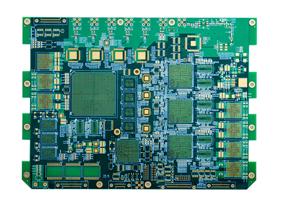
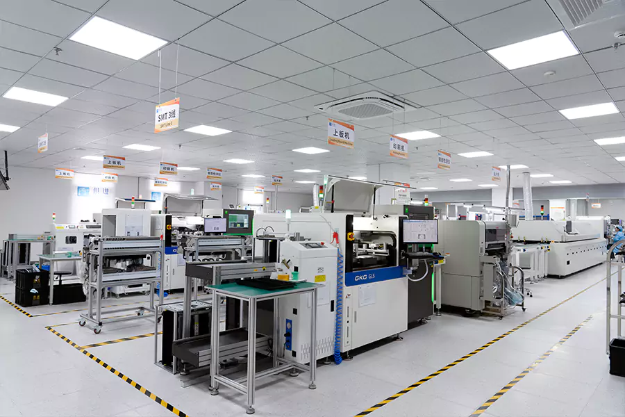
Multilayer printed circuit boards (PCBs) are essential for high-density, high-speed, and space-constrained applications. They consist of alternating layers of conductive copper and insulating dielectric materials laminated together under heat and pressure to form a single, unified board. While the overall process involves many steps, this section provides a high-level view of the critical stages in multilayer PCB manufacturing to help contextualize where inner layer imaging and lamination fit within the full fabrication cycle.
Key Stages in Multilayer PCB Manufacturing
- Core Preparation
The process begins with copper-clad laminates (core materials), which serve as the building blocks for inner layers. These cores are cleaned and treated to ensure proper adhesion and photoresist coating in the following steps. - Inner Layer Patterning
Inner layers undergo imaging and etching processes to define the required circuit patterns. This involves photoresist application, UV exposure using artwork or LDI, chemical development, and precise copper etching. - Oxide Treatment / Surface Conditioning
Before lamination, the inner layers are chemically treated to promote strong adhesion during the lamination process. This step enhances bond strength and reduces the risk of delamination. - Lay-Up and Lamination
The patterned inner layers are stacked together with layers of prepreg (resin-impregnated fiberglass) and additional copper foil, arranged according to the board’s stack-up design. This assembly is then laminated in a press under controlled heat and pressure to bond the layers into a single structure. - Drilling and Plating
After lamination, holes are drilled to create vias and through-holes, followed by electroless and electroplating processes to establish electrical connections between layers. - Outer Layer Imaging and Etching
Similar to the inner layers, the outer copper layers are patterned using photoresist, exposure, and etching techniques to define traces and pads. - Solder Mask, Surface Finish, and Silkscreen
Protective solder mask is applied over the circuitry, followed by surface finishes (ENIG, HASL, OSP, etc.) to enhance solderability and reliability. Silkscreen is then printed for component labeling. - Electrical Testing and Final Inspection
The finished boards undergo rigorous electrical testing, dimensional inspection, and quality assurance checks to ensure they meet design and IPC standards.
Inner-Layer Circuit Pattern Imaging
The process of inner-layer imaging is a critical step in multilayer PCB fabrication. It defines the conductive traces on each internal layer before lamination, and any deviation at this stage can cascade into registration errors, signal integrity issues, or final board rejection. This section outlines the key stages involved in accurately transferring and developing circuit patterns onto inner copper cores.
1. Copper Core Preparation
Before image transfer, the copper-clad laminate (core) must be meticulously cleaned. This ensures proper adhesion of photoresist and minimizes the risk of contamination defects. The cleaning process usually involves:
- Brushing and micro-etching to remove oxidation and surface debris
- Deionized water rinsing to eliminate chemical residues
- Drying in a cleanroom environment to prevent recontamination
Proper surface preparation enhances photoresist adhesion and ensures uniform exposure across the panel.
2. Photoresist Application
A layer of photoresist, typically dry film, is laminated onto the copper surface using heat and pressure. Dry film is preferred for its uniform thickness and resolution consistency. In some advanced facilities, liquid photoresist may be used for fine-line imaging in HDI boards.
Key parameters during lamination include:
- Lamination temperature (typically 105–120 °C)
- Roller pressure and speed
- Film thickness (commonly 30–50 μm)
These must be tightly controlled to ensure good edge coverage and to avoid trapped air bubbles or wrinkles, which could lead to imaging defects.
3. UV Exposure (Imaging)
Once laminated, the panel is exposed to ultraviolet (UV) light through a photomask that defines the desired circuit pattern. This is typically performed using:
- Contact exposure systems for standard resolution
- Laser Direct Imaging (LDI) systems for finer pitch, faster setup, and greater accuracy
During exposure, the UV light alters the solubility of the photoresist: in positive photoresist, the exposed areas become soluble and will be removed in developing; in negative resist, the exposed areas become insoluble and remain to protect the copper.
Proper exposure alignment (registration) is crucial to ensure that each layer aligns correctly with the others during final stack-up. Fiducials and alignment pins are often used to achieve sub-25 μm precision.
4. Developing and Etching
After exposure, the panel goes through a developing process, typically using a mild alkaline solution that washes away the soluble resist. This leaves the copper layer selectively protected by the remaining hardened resist.
Next, the panel undergoes acidic or alkaline etching, depending on the copper type and process requirements:
- Acidic etchants (e.g., ferric chloride, cupric chloride) are common for high-volume production
- Alkaline etchants (e.g., ammoniacal solutions) offer higher etch rates and better control for fine-line geometries
Etching removes all exposed copper, leaving behind the circuit traces protected by the photoresist. After etching, the remaining resist is stripped off in a final cleaning step, exposing the finished copper circuitry.
5. Automatic Optical Inspection (AOI)
To verify the integrity of each inner-layer pattern before lamination, the core is subjected to Automatic Optical Inspection (AOI). This non-contact process uses high-resolution cameras and pattern-recognition algorithms to detect:
- Open circuits
- Shorts between traces
- Over-etching or under-etching
- Misregistration of pads or vias
AOI is a critical quality control gate and helps avoid costly errors during the lamination phase. If defects are found, panels may be scrapped or reworked depending on severity and company policy.
Material Shrinkage & Scaling Compensation
Understanding Material Shrinkage During Lamination
During the lamination process of multilayer PCBs, the prepreg and core materials undergo significant thermal and mechanical stress. As the stack-up is subjected to elevated temperatures and pressure, materials expand and contract—leading to dimensional changes that can misalign inner-layer circuitry. This dimensional instability is commonly referred to as material shrinkage or registration distortion.
Prepreg resin flows and cures during hot pressing, causing uneven contraction depending on fiber weave, resin content, and lamination profiles. Core materials (pre-cured fiberglass with copper) also respond to heat, especially across large panel sizes. Typical shrinkage values range from 0.05% to 0.2%, or 500 to 2000 ppm, and may vary between X and Y axes due to glass fabric orientation.
Uncompensated shrinkage can lead to:
- Inner-layer misregistration
- Warped stack-ups
- Misaligned vias or pad-to-trace mismatches
- Reduced layer-to-layer reliability
Key Factors Influencing Shrinkage
Several variables influence the amount and direction of shrinkage during lamination:
- Material Type: Different prepregs and cores (e.g., FR-4 vs. polyimide) have different coefficients of thermal expansion (CTE).
- Copper Density & Distribution: Uneven copper coverage across layers can cause differential heating and distortion.
- Lamination Cycle Parameters: The heating rate, peak temperature, dwell time, pressure, and cooling rate all impact dimensional stability.
- Panel Size & Shape: Larger panels tend to exhibit more noticeable shrinkage, particularly near edges.
Design-Time Scaling Compensation
To counteract expected shrinkage, manufacturers apply scaling factors to the inner-layer artwork during the phototooling stage. This means intentionally oversizing or undersizing the artwork so that after lamination, the final dimensions align within tolerance.
Common Scaling Techniques:
- Global Scaling: Apply a uniform percentage to the entire image (e.g., scale by +0.08% in X, +0.05% in Y).
- Axis-Specific Scaling: Compensate for anisotropic shrinkage due to fabric weave (e.g., 0.07% in X-axis, 0.10% in Y-axis).
- Zone-Based Compensation: Advanced CAM tools adjust different zones of the panel independently, accounting for localized copper density and historical panel behavior.
Data-Driven Compensation with Historical Panels
Modern PCB fabricators use statistical process control (SPC) and historical panel shrinkage data to fine-tune scaling factors for each material stack-up. By measuring actual post-lamination shrinkage across many panels and layer counts, they can build shrinkage profiles to automatically apply scaling with higher accuracy.
Best Practices for Designers
While scaling is handled by the manufacturer, designers can support accurate compensation by:
- Keeping copper density balanced across the panel to reduce distortion
- Using symmetrical stack-ups for consistent shrinkage behavior
- Communicating stack-up intent early in the design to help fabricators apply the correct scaling profiles
- Avoiding dense copper features close to the panel edge, where distortion is typically higher
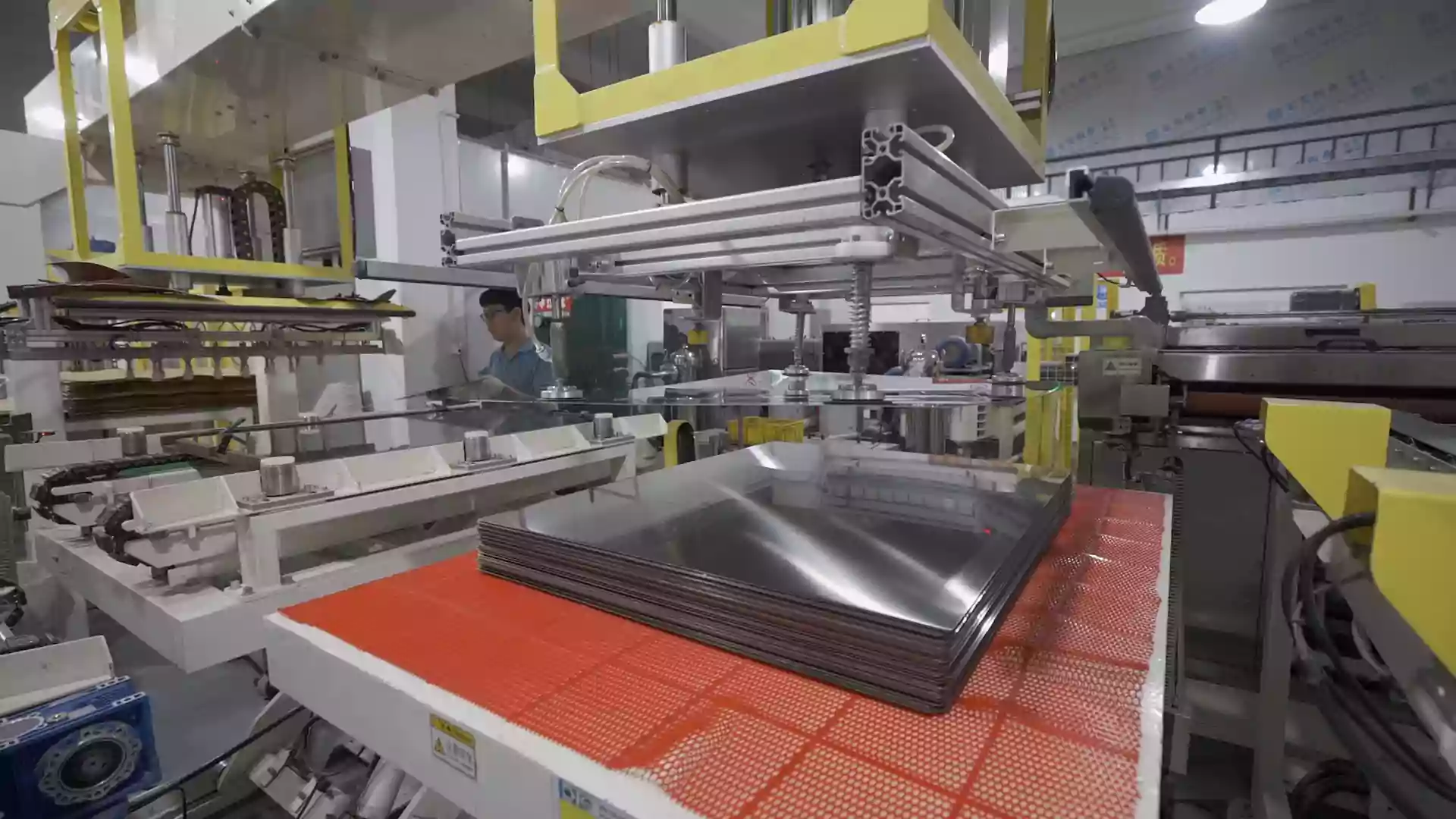
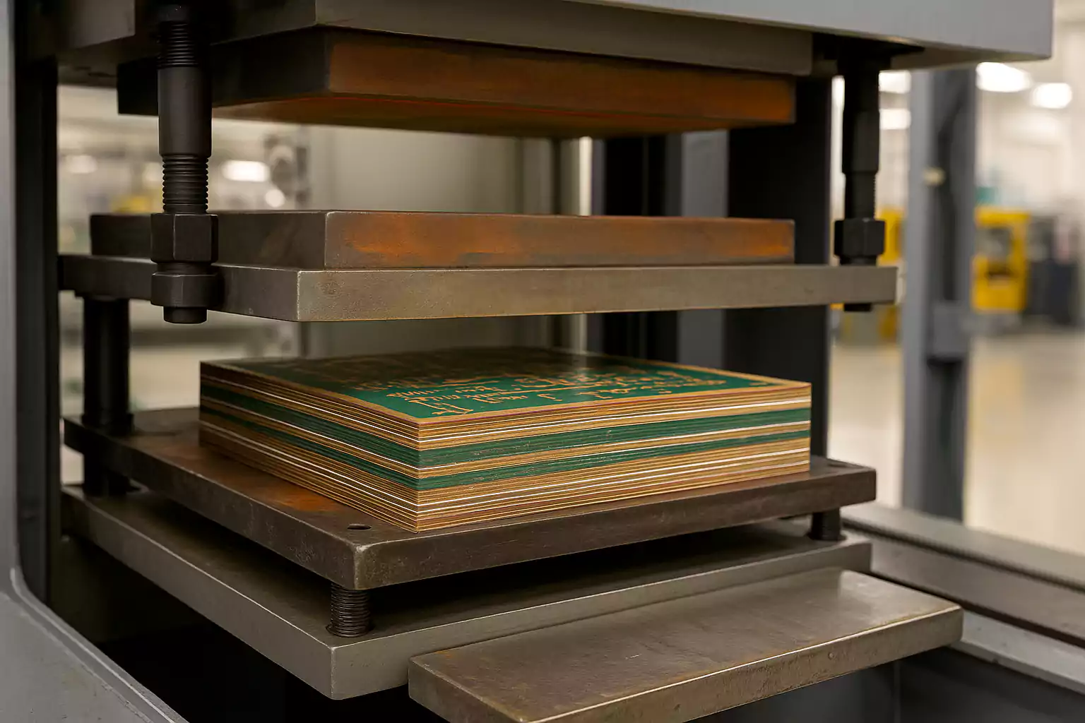
Lay-Up & Lamination Details
Lamination is the core process that transforms separate inner layer cores and prepregs into a mechanically bonded, electrically unified multilayer PCB. This section explores the key steps and considerations involved in the lamination process, including lay-up preparation, press cycle optimization, and defect prevention.
1.Lay-Up Preparation
Before pressing, the PCB manufacturer performs a lay-up operation in a cleanroom environment to ensure alignment accuracy and contamination control. The lay-up stack typically consists of:
- Inner layer cores (pre-etched and AOI-inspected)
- Prepreg sheets (uncured resin layers that will bond the stack)
- Copper foil (for outer layers, if applicable)
- Release films and separator plates (to prevent sticking and ensure smooth pressure distribution)
To maintain layer-to-layer registration, alignment pins or optical registration systems are used. It is essential to mirror and alternate copper features to achieve a balanced stack-up, which minimizes stress and warpage during lamination. Misaligned lay-up is one of the top contributors to via misregistration and inner-layer offset.
2.Lamination Press Cycle: Heat, Pressure, Time
Once lay-up is complete, the stack is loaded into a hydraulic or vacuum-assisted lamination press. The lamination cycle is controlled by three critical variables:
- Temperature Ramp-Up: Gradually heating to the resin's flow point (typically 170–190°C) allows even resin distribution.
- Pressure Application: Controlled pressure (around 200–300 psi) ensures proper adhesion and resin filling of microgaps between layers.
- Dwell Time: A hold period at peak temperature and pressure ensures complete resin cure and bonding. This usually ranges from 60 to 90 minutes, depending on material specifications.
The cool-down phase must be slow and uniform to prevent delamination or warping. Sudden temperature drops can cause internal stresses and voids in the laminate.
3.Vacuum Lamination: Enhancing Bond Integrity
Many advanced PCB fabricators adopt vacuum lamination to remove trapped air and reduce the risk of voids or delamination. By applying a vacuum before and during the heating phase, gas bubbles are eliminated, which improves:
- Resin wetting and flow
- Inner layer adhesion
- Dielectric consistency
Vacuum lamination is especially beneficial when using low-flow prepregs, fine-pitch designs, or large panel sizes where trapped gases can compromise electrical integrity.
4.Common Lamination Defects and Process Control
Poor control during lamination can lead to structural and functional issues such as:
| Defect | Cause | Prevention |
|---|---|---|
| Delamination | Incomplete cure, trapped moisture, poor prepreg | Pre-bake materials, control dwell time |
| Resin voids | Trapped air, inadequate pressure | Use vacuum lamination, optimize ramp-up |
| Warpage | Asymmetrical stack-up, uneven cooling | Design for symmetry, control cooling rate |
| Inner-layer shift | Poor registration or excessive press pressure | Use optical registration, balanced lay-up |
To minimize defects, manufacturers often conduct cross-sectional analysis, X-ray inspection, and resin coverage tests post-lamination to verify structural integrity before drilling and outer layer processing.
5.Material Behavior Under Press Conditions
Prepregs are heat-sensitive and behave differently depending on their resin content and glass weave type. During lamination:
- Resin must flow sufficiently to fill voids and wet copper surfaces but not excessively to avoid resin starvation.
- The glass transition temperature (Tg) of the material must be exceeded to allow full polymer crosslinking.
- Pressure must be optimized to avoid over-compression, which can thin out dielectric spacing and increase capacitance.
Understanding the rheology of the resin system (i.e., how it flows under heat and pressure) is critical for reliable lamination. Material data sheets typically provide processing windows, but experienced engineers often fine-tune profiles based on empirical data and product complexity.
Thickness, Tolerance & Reliability
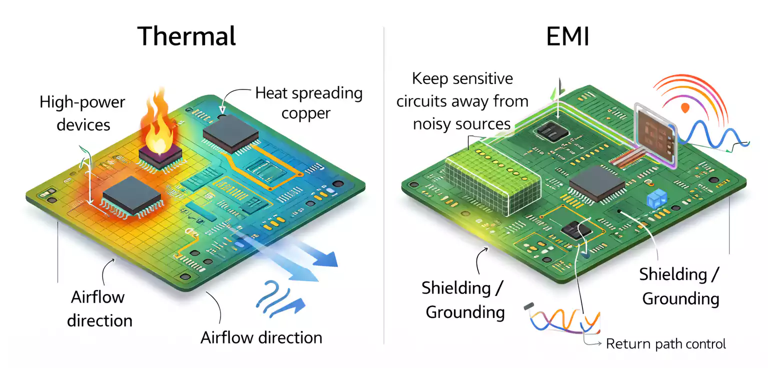
When manufacturing multilayer PCBs, the total board thickness and its associated tolerances are more than just dimensional specs—they play a critical role in electrical performance, thermal behavior, mechanical strength, and overall product reliability. Understanding how these factors interconnect allows engineers to make better design decisions and avoid costly rework or failure.
1.Understanding Total PCB Thickness
The final thickness of a PCB is the result of layering cores, prepregs, and copper foils—each contributing to the overall stack-up. Standard board thicknesses range from 0.4 mm to 3.2 mm, with 1.6 mm being the most common in commercial applications. The thickness is influenced by:
- Number of layers and dielectric materials used
- Type and thickness of copper (e.g., 1 oz vs 2 oz)
- Prepreg resin flow and squeeze-out during lamination
- Pressing parameters such as temperature, pressure, and dwell time
If not properly controlled, deviations in these variables can result in uneven dielectric spacing, impedance mismatches, and mechanical deformation.
2.Tolerance Standards and Real-World Impacts
PCB manufacturers typically aim for a thickness tolerance of ±10%, although high-reliability applications may demand tighter tolerances (e.g., ±0.05 mm or even lower for HDI or RF designs).
Failing to meet the specified tolerance can lead to several issues:
- Signal Integrity Problems: Variations in dielectric spacing affect impedance, potentially disrupting high-speed or RF performance.
- Via Reliability Risks: Changes in board thickness can alter via aspect ratios, increasing the chance of barrel cracking during thermal cycling.
- Mechanical Fitment Issues: PCBs may not fit properly in enclosures or connectors, especially in stacked assemblies or products with tight packaging constraints.
- Thermal Expansion Mismatch: Boards with uneven thickness may exhibit localized stress or warpage under thermal load.
3.The Role of Layer Symmetry and Stack-Up Balance
Reliable PCBs require a symmetrical and balanced stack-up to prevent bow and twist after lamination. Uneven thickness across layers—either due to mismatched core materials or inconsistent prepreg usage—can cause deformation that compromises both mechanical and electrical performance.
Design engineers should coordinate closely with fabricators to ensure the following:
- Prepregs are placed evenly across the stack-up
- Copper weight distribution is symmetrical
- Total dielectric thickness is consistent between top and bottom halves
- Resin content is sufficient to fill internal voids without over-squeeze
4.Optimizing Thickness for Product Reliability
Selecting the appropriate board thickness is a balancing act between mechanical strength, thermal management, and electrical integrity. For example:
- Thicker boards (≥2.0 mm) offer increased rigidity and current-carrying capacity but may be prone to warpage and thermal stress.
- Thinner boards (≤1.0 mm) allow compact designs and better thermal dissipation but may require additional support during assembly or operation.
When optimizing for reliability, consider:
- The environment (e.g., automotive vs consumer electronics)
- Expected mechanical loads (e.g., vibration, bending)
- Thermal cycling range and duration
- Critical signal paths and impedance control zones
5.Manufacturing Best Practices
To achieve tight thickness control and enhance product reliability:
- Use controlled-flow prepregs with well-defined resin content
- Implement pre-bake routines to remove moisture from laminates
- Apply real-time press monitoring to adjust for resin flow variability
- Specify board thickness targets and tolerances clearly in the fabrication notes and Gerber files
- Conduct cross-section analysis and flatness tests post-lamination to verify results
Design and Manufacturing Recommendations
To ensure successful multilayer PCB fabrication—especially during inner layer imaging and lamination—engineers must apply a holistic “Design for Manufacturability” (DFM) approach. Below are practical recommendations that bridge design intent with process capabilities, minimizing production risks and enhancing long-term reliability.
1.Collaborate Early with Your PCB Manufacturer
Involve your fabrication partner early in the design phase to discuss:
- Stack-up feasibility and preferred prepreg/core configurations
- Material compatibility and availability
- Registration tolerances and expected shrinkage factors
- Minimum trace/space rules based on imaging and etching precision
Early DFM collaboration helps identify constraints before layout, preventing costly redesigns and delays.
2.Balance the Stack-Up
Always design for mechanical and thermal symmetry:
- Use mirrored layer pairs (e.g., L1–L8 vs L2–L7)
- Distribute copper weight evenly across layers to avoid warpage
- Choose symmetrical dielectric thickness and resin flow paths
An imbalanced stack-up can cause bowing, delamination, or misregistration during lamination and cooling.
3.Scale for Material Shrinkage
Account for dimensional changes during lamination by:
- Applying accurate X-Y scaling to inner layers based on known material properties (typically 500–1000 ppm)
- Consulting your fabricator’s historical shrinkage data
- Testing with pilot panels if using new materials or large board formats
Failure to scale inner layers properly leads to poor registration and misaligned vias.
4.Optimize for Imaging and AOI
Ensure that your design:
- Incorporates fiducials and tooling holes for accurate layer alignment
- Avoids ultra-dense patterns near panel edges (prone to under-etch or exposure drift)
- Includes clear solder mask clearance around traces and vias for AOI effectiveness
A clean imaging and inspection process reduces defects like underexposure, over-etching, or misaligned traces.
5.Standardize Core and Prepreg Combinations
Stick to commonly used combinations (e.g., 2116 + 7628 prepregs with standard FR-4 core thicknesses) to:
- Ensure better lamination consistency
- Achieve predictable dielectric spacing and impedance
- Reduce lead time and sourcing risk
Non-standard stack-ups often require special tooling or test runs, adding cost and time.
6.Control Finished Thickness and Copper Balance
Design with total finished thickness in mind:
- Meet IPC-2221 or product-specific requirements
- Adjust copper layer thicknesses to stay within manufacturing capabilities (e.g., 1 oz/ft² vs 2 oz)
- Use copper thieving patterns to maintain uniformity in copper distribution and prevent resin starvation
This improves lamination pressure distribution and helps maintain target thickness tolerances.
7.Prepare for Reliability Testing
For high-reliability applications (e.g., automotive, aerospace, medical):
- Design for thermal stress endurance, considering z-axis expansion
- Choose low-CTE or high-Tg materials
- Request cross-section analysis or microsection coupons to validate inner layer bonding and resin fill
These design provisions improve lifetime performance under thermal cycling and mechanical stress.
Troubleshooting Common Issues in Inner Layer Imaging and Lamination
| Issue | Possible Causes | Impact on PCB | Recommended Solutions |
|---|---|---|---|
| Inner Layer Misregistration | - Inaccurate tooling or pin alignment- Improper scaling compensation- Material movement during lamination | - Misaligned vias- Short circuits or open traces between layers | - Use optical targets and registration punches- Adjust scaling based on real shrinkage data- Implement layer-to-layer registration verification (e.g., X-ray) |
| Delamination After Lamination | - Excessive moisture in prepreg or core- Inadequate lamination pressure/temperature- Oxidized copper surfaces | - Reduced mechanical strength- Electrical discontinuities- Board failure during reflow | - Pre-bake materials at 105–125 °C for 4–6 hours- Optimize lamination pressure/temp profiles- Apply oxide/oxide alternative treatments |
| Resin Voids Between Layers | - Insufficient resin flow- Incorrect prepreg selection or stack-up imbalance- Entrapped air due to poor lay-up | - Reduced dielectric strength- Risk of electrical arcing or failure under stress | - Use adequate resin content prepregs- Optimize press cycle and dwell time- Apply vacuum lamination if needed |
| Etching Undercut or Over-Etch | - Overexposure in photoresist- Uncontrolled etchant temperature/concentration- Uneven resist coating | - Reduced trace width- Risk of trace breaks or signal degradation | - Calibrate exposure energy and time- Maintain stable etchant chemistry and flow- Ensure even dry film lamination |
| Image Shift or Blurring | - Dirty or scratched artwork- Misaligned phototools or LDI setup- Vibration during exposure | - Trace distortion- Increased impedance variation or cross-talk | - Clean phototools before each use- Use rigid setups and anti-vibration platforms- Validate alignment with test panels |
| Copper-to-Dielectric Separation | - Inadequate oxide treatment- Poor surface prep- Lamination underpressure | - Poor peel strength- High risk of delamination in thermal cycling | - Improve surface roughening or micro-etching- Use verified oxide chemistries- Increase lamination pressure within material limits |
| Board Warpage Post-Lamination | - Asymmetrical stack-up- Inconsistent heating/cooling rates- Improper core/prepreg combination | - Handling issues- Drill misalignment- Incompatibility with SMT processes | - Ensure symmetrical stack-ups- Control lamination ramp rates- Use matched material systems with similar CTE |
| Pinholes or Pitting in Copper Layers | - Contamination during imaging- Incomplete resist coverage- Etchant attack on exposed areas | - Increased risk of shorts or corrosion- Lower surface finish reliability | - Improve cleanroom conditions- Inspect resist application quality- Use conformal dry films with better edge coverage |
Conclusion
Inner layer imaging and lamination are critical to the precision and reliability of multilayer PCBs. These stages influence registration accuracy, dimensional stability, and electrical performance.
As board complexity increases, small process deviations can lead to major failures. Designers should collaborate with manufacturers early to align on scaling factors, material behavior, and stack-up symmetry. Engineers must rely on precise process controls to avoid defects like warpage or delamination.
By understanding the interdependence of imaging and lamination, teams can improve fabrication yield, ensure signal integrity, and build robust boards for demanding applications.