


Introduction
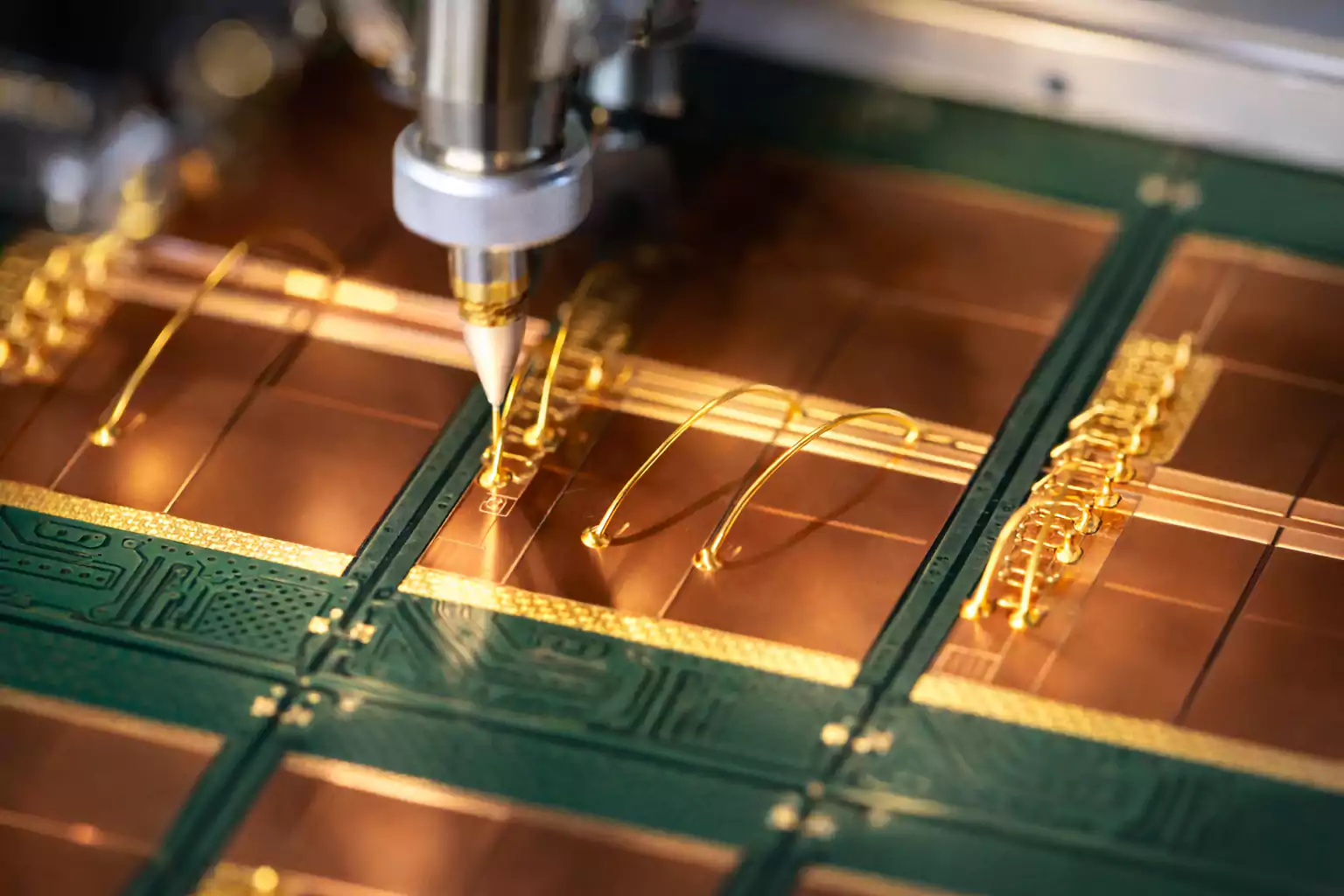
In surface mount technology (SMT) assembly, the solder paste printing process plays a critical role in determining overall product quality and manufacturing yield. Even with high-precision placement and reflow equipment, poor solder paste application can lead to defects such as bridging, insufficient solder, or misalignment—issues that are difficult to correct later in the process.
To address these challenges early, manufacturers increasingly rely on Solder Paste Inspection (SPI) systems. Positioned directly after the printing stage, SPI serves as a crucial quality gate, allowing for real-time detection and correction of print-related defects before components are mounted.
As electronics continue to shrink and PCB designs grow more complex, traditional inspection methods often fall short. That’s where 3D SPI comes in—offering greater accuracy, full-volume analysis, and the ability to drive measurable improvements in first-pass yield and long-term reliability.
This article explores what SPI is, how 3D SPI differs from 2D systems, and why it has become an essential tool for high-reliability SMT production.
What Is Solder Paste Inspection (SPI)?
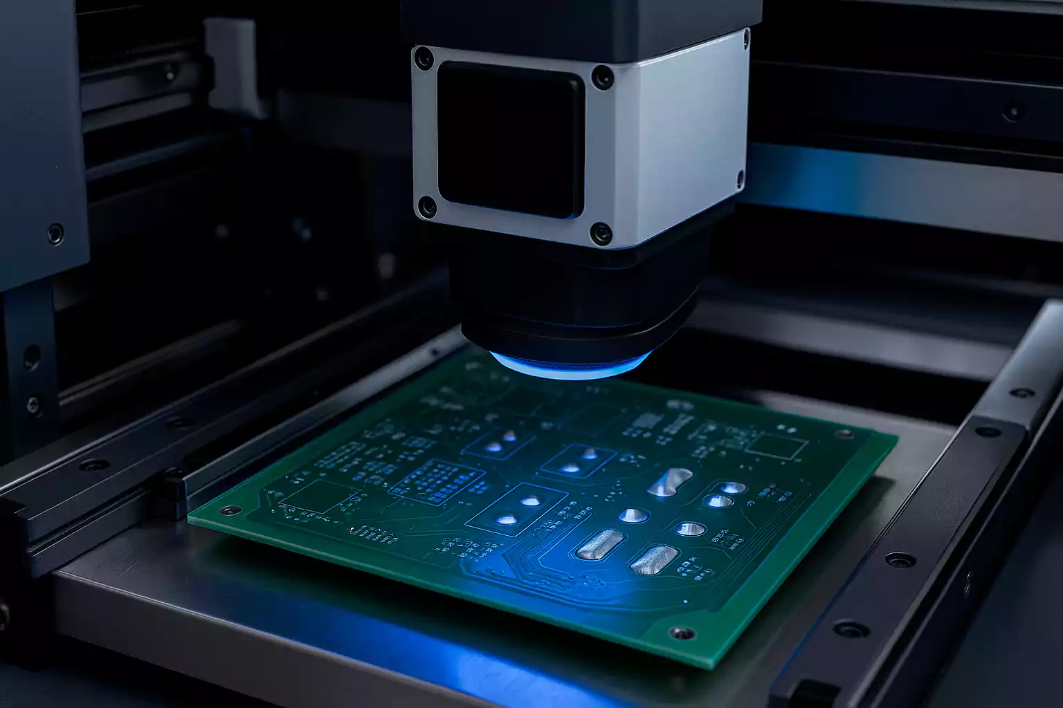
Solder Paste Inspection (SPI) is an automated process used to evaluate the quality and consistency of solder paste deposits on a printed circuit board (PCB) immediately after stencil printing. It acts as a critical quality control checkpoint in SMT (Surface Mount Technology) assembly, helping manufacturers catch print-related defects before components are placed and reflowed.
How SPI Works
SPI systems use high-resolution cameras and structured light to scan each solder pad on the PCB. The inspection system then reconstructs a 2D or 3D image of each deposit and compares it to predefined reference values. Key parameters measured include:
- Volume: Total solder paste deposited on the pad
- Height: Vertical thickness of the paste
- Area: Surface coverage on the pad
- Offset / Alignment: Deviation from the pad center
- Shape / Contour: Uniformity and geometry of the paste
- Bridging / Short detection: Whether paste overlaps adjacent pads
Why SPI Matters in SMT
SPI plays a preventive role in ensuring that solder joints will form correctly during reflow. Poor solder paste application is one of the leading causes of soldering defects, including open circuits, tombstoning, bridging, and cold joints. By catching these issues early—before placement—SPI reduces scrap, rework, and costly downstream failures.
Additionally, SPI systems provide statistical data that can be used to fine-tune the stencil design, printing process, and environmental conditions, enabling continuous process improvement (CPI) in high-volume manufacturing.
3D SPI vs 2D SPI – Technical Comparison and Advantages
As PCB designs become denser and component packages more complex, accurate solder paste inspection becomes increasingly critical. While traditional 2D SPI systems have served manufacturers for years, 3D SPI has emerged as a superior solution for modern SMT production lines. Below is a breakdown of how 3D SPI differs from 2D SPI in terms of technology, capabilities, and impact on quality.
2D SPI: Limited Surface Analysis
2D SPI systems rely on grayscale image processing or simple laser triangulation to inspect the solder paste surface. They primarily measure:
- Surface area
- Position of paste deposits
- Outline or silhouette of the printed paste
While effective for basic inspection, 2D systems struggle to accurately detect height, volume, or subtle variations in paste shape—especially on fine-pitch components or densely populated boards.
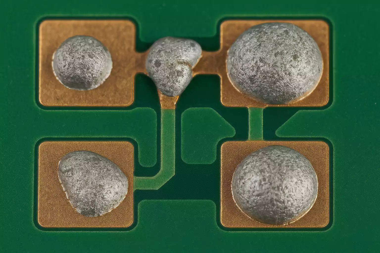
3D SPI: Full Volume Measurement
3D SPI uses advanced structured light projection and multi-angle imaging to reconstruct a true three-dimensional model of each solder deposit. It measures all critical dimensions, including:
- Paste volume (key for joint reliability)
- Height profile
- Base area and spread
- Offset and tilt
- Shape irregularities and surface anomalies
This comprehensive data allows for more precise defect detection, better process control, and a significant reduction in false calls and missed defects.
Key Advantages of 3D SPI Over 2D SPI
| Feature | 2D SPI | 3D SPI |
|---|---|---|
| Volume Measurement | No | Yes (accurate volumetric data) |
| Height Detection | Limited | Full Z-axis resolution |
| Detection of Shape Defects | Basic silhouette analysis | Detailed contour mapping |
| Fine-pitch Compatibility | Less reliable | High accuracy for tight tolerances |
| False Call Reduction | Higher | Lower false alarms with true 3D data |
| Process Feedback | Limited insights | Granular SPC and real-time feedback |
Why 3D SPI Matters
The ability to measure paste volume is one of the most impactful benefits of 3D SPI. Volume directly affects the formation of reliable solder joints. Too little paste can cause open connections, while excess paste increases the risk of bridging and tombstoning.
By capturing this data in real time, 3D SPI enables manufacturers to identify trends, correct stencil or printer issues, and fine-tune their process before defects propagate.
How 3D SPI Improves SMT Yield and Quality
Implementing 3D Solder Paste Inspection (SPI) is one of the most effective ways to enhance surface mount technology (SMT) assembly yield and overall product quality. By providing accurate, real-time feedback on solder paste deposition, 3D SPI helps manufacturers prevent defects early, minimize rework, and improve first-pass yield (FPY).
1. Early Detection of Critical Defects
Most SMT defects—such as bridging, tombstoning, insufficient solder, or component misalignment—originate from poor solder paste printing. 3D SPI detects these issues immediately after the printing process by analyzing:
- Paste volume consistency
- Paste height and coverage
- Offset from pad center
- Abnormalities in shape or tilt
This early-stage detection prevents defective boards from reaching the placement or reflow stages, where problems become harder and more expensive to fix.
2. Enhanced First-Pass Yield (FPY)
First-pass yield refers to the percentage of PCBs that pass all inspection and test stages without requiring rework. With 3D SPI in place, manufacturers can:
- Identify trends or systematic print issues (e.g., worn stencils, improper alignment)
- Continuously monitor process drift and correct it in real time
- Reduce false calls and unnecessary manual inspections
Improving FPY reduces total production time, lowers labor costs, and ensures more consistent product output.
3. Closed-Loop Feedback and Process Control
Modern 3D SPI systems can be integrated into closed-loop feedback systems with stencil printers. When an out-of-tolerance condition is detected, the SPI system can trigger automatic printer adjustments or alerts to operators. This dynamic control helps:
- Maintain optimal print conditions
- Compensate for environmental or mechanical shifts
- Minimize downtime due to manual recalibration
Such proactive control stabilizes the printing process and improves line efficiency over time.
4. Support for High-Density and Fine-Pitch Designs
With the growing adoption of fine-pitch components, micro-BGAs, and high-density interconnect (HDI) PCBs, paste deposition accuracy becomes more critical. 3D SPI offers the resolution and precision needed to:
- Ensure correct volume on very small pads
- Detect bridging or overflow between closely spaced pads
- Maintain compliance with tight tolerances required for advanced electronics
This makes 3D SPI especially valuable in sectors like automotive, aerospace, and medical electronics, where quality and reliability are non-negotiable.
5. Data-Driven Quality Improvements
3D SPI systems provide rich statistical process control (SPC) data that can be used for:
- Root cause analysis of defects
- Continuous improvement (CPI) initiatives
- Long-term process optimization
Common Defects Detected by SPI
Solder Paste Inspection (SPI) systems are designed to catch a wide range of solder paste printing defects that directly impact the quality and reliability of surface mount assemblies. Identifying these issues early in the SMT process not only prevents costly rework but also ensures consistent solder joint formation during reflow.
Below are the most common defects detected by 3D SPI systems, along with their causes and potential consequences.
1. Insufficient Solder Paste
Description: The volume or height of solder paste is below the required specification.
Causes:
- Clogged or worn stencil apertures
- Inadequate squeegee pressure
- Low viscosity solder paste
Consequences: - Weak or open solder joints
- Increased risk of intermittent electrical failures
2. Excess Solder Paste
Description: Too much solder paste is deposited on the pad.
Causes:
- Oversized stencil apertures
- Excessive paste volume settings
- Misaligned stencil or overprinting
Consequences: - Bridging between adjacent pads
- Tombstoning of small components
- Voiding or solder ball formation during reflow
3. Paste Misalignment (Offset Printing)
Description: The solder paste deposit is not centered on the pad.
Causes:
- Stencil misalignment
- PCB or stencil slippage during print
- Incorrect board registration
Consequences: - Component placement issues
- Weak or incomplete solder joints
- Bridging or open circuits
4. Bridging
Description: Solder paste connects two or more adjacent pads unintentionally.
Causes:
- Excess paste volume
- Narrow pad spacing (fine pitch)
- Stencil design flaws
Consequences: - Electrical shorts
- Complete board failure if undetected
5. Smearing or Slumping
Description: Paste spreads beyond the pad area or loses its defined shape.
Causes:
- Incorrect stencil separation speed
- Low paste viscosity or expired paste
- Improper environment (temperature, humidity)
Consequences: - Solder shorts or irregular joints
- Voiding under components
6. Paste Height Variation
Description: Inconsistent height across similar pads or deposits.
Causes:
- Uneven stencil contact
- Inconsistent squeegee pressure or angle
- Warped PCB or stencil
Consequences: - Inconsistent reflow behavior
- Variable joint quality and reliability
7. No Paste (Missing Print)
Description: One or more pads are completely missing solder paste.
Causes:
- Blocked stencil aperture
- Skipped print cycle
- Printer malfunction
Consequences: - Open solder joints
- Component placement failure
Implementation Best Practices and Equipment Selection
Successfully deploying a 3D Solder Paste Inspection (SPI) system requires more than just purchasing the right machine. To fully leverage its capabilities and maximize ROI, manufacturers must align SPI implementation with stencil design, solder paste characteristics, printing process settings, and ongoing maintenance routines. Below are the key best practices and equipment selection criteria for optimizing SPI performance in SMT assembly.

1. Select the Right 3D SPI Equipment
Not all 3D SPI systems are created equal. When evaluating equipment options, consider the following specifications:
- Measurement Accuracy & Repeatability: Look for systems with sub-micron Z-axis resolution and consistent repeatability across the PCB surface.
- Inspection Speed: Choose a system that balances speed and accuracy, especially for high-throughput production lines.
- Field of View (FOV): A larger FOV enables faster inspection of multiple pads or components simultaneously.
- Lighting and Projection Technology: Structured light, Moiré fringe, and dual-projection systems offer better 3D reconstruction.
- Software Capabilities: Ensure the system provides user-friendly programming, SPC data collection, trend analysis, and closed-loop feedback integration.
Top vendors such as Koh Young, Omron, CyberOptics, and Mirtec offer robust 3D SPI solutions for various production environments.
2. Calibrate and Maintain the System Regularly
Ongoing calibration and maintenance are critical for maintaining inspection accuracy. Best practices include:
- Daily Calibration using manufacturer-provided tools or reference boards
- Lens and sensor cleaning to prevent optical errors
- Routine software updates for enhanced defect detection algorithms
- Environmental control (temperature, lighting) to ensure measurement consistency
Establishing a preventive maintenance schedule will reduce downtime and maintain optimal performance.
3. Align SPI with Stencil and Printer Design
SPI should not be treated as a stand-alone system. It must integrate seamlessly with your solder paste printing process:
- Stencil Design: Ensure aperture size, shape, and stencil thickness align with board design and paste volume requirements.
- Stencil Quality: Use laser-cut, nano-coated stencils to reduce clogging and ensure clean paste release.
- Printer Compatibility: Verify that your SPI system can exchange data with the stencil printer for closed-loop control.
Implementing design-for-inspection (DFI) principles during PCB and stencil design can significantly reduce false calls and enhance inspection coverage.
4. Set Accurate Tolerances and Thresholds
Avoid setting SPI tolerances too tightly or too loosely. Overly strict thresholds can lead to false rejects, while loose settings may allow critical defects to pass undetected. Best practices include:
- Use IPC guidelines (e.g., IPC-7527) as a starting point
- Tailor thresholds based on pad size, pitch, and component type
- Continuously review defect trends to fine-tune thresholds over time
5. Use SPI Data for Process Improvement
A major advantage of 3D SPI systems is their ability to collect real-time SPC (Statistical Process Control) data. Leverage this data to:
- Identify recurring process issues (e.g., worn squeegees, stencil clogging)
- Monitor Cp/Cpk process capability indices
- Optimize paste type, print pressure, and separation speed
- Detect gradual performance drift before defects escalate
Continuous improvement driven by SPI insights can yield long-term gains in yield and quality.
Future Trends in SPI
As electronics manufacturing continues to evolve, Solder Paste Inspection (SPI) is no longer just a checkpoint for detecting print defects—it is becoming a central driver of smart, connected, and fully automated production lines. The following trends highlight how SPI technology is expected to advance in the coming years.
1. AI-Driven Defect Recognition
Artificial intelligence and machine learning are increasingly being integrated into SPI systems to improve defect classification. Instead of relying solely on fixed thresholds, AI algorithms can learn from large datasets of images, reducing false calls and improving detection of subtle or complex defects. This adaptive approach allows SPI systems to “get smarter” over time and adjust to changing process conditions.
2. Real-Time Closed-Loop Control
Next-generation SPI systems are designed to work in real time with stencil printers and placement machines. When an out-of-tolerance condition is detected, the system can automatically adjust printer parameters—such as squeegee pressure or stencil alignment—without operator intervention. This closed-loop feedback ensures consistent solder paste volume and alignment, improving first-pass yield and reducing downtime.
3. Integration With Industry 4.0 and Smart Factories
In modern manufacturing, SPI systems are evolving into data hubs. By connecting with Manufacturing Execution Systems (MES) and Enterprise Resource Planning (ERP) platforms, SPI data can be analyzed alongside other process metrics. This integration supports:
- Predictive maintenance: identifying equipment wear before it impacts quality
- Process traceability: capturing full inspection records for each board
- Automated decision-making: enabling lights-out manufacturing in highly automated lines
4. Higher Resolution for Miniaturization
With the rise of 0201 components, micro-BGAs, and advanced HDI boards, inspection accuracy requirements are tighter than ever. Future SPI systems will feature higher optical resolution, finer fringe projection patterns, and improved Z-axis accuracy to ensure reliable measurement of ultra-small pads.
5. Cloud and Big Data Analytics
As manufacturers adopt digital transformation strategies, SPI data is increasingly stored and analyzed in the cloud. This enables multi-site comparisons, benchmarking, and predictive analytics across global production lines. Leveraging big data also helps optimize material usage, identify systemic weaknesses, and support continuous improvement initiatives.
6. Hybrid Inspection Approaches
Emerging solutions combine SPI with other inspection technologies such as Automated Optical Inspection (AOI) and X-ray. By merging different datasets, manufacturers can gain a more comprehensive view of process health—from solder paste printing to placement and reflow.
Conclusion
Solder Paste Inspection (SPI) has evolved into a critical quality gate in surface mount technology (SMT) assembly, ensuring that defects originating from the printing process are identified and corrected before they compromise downstream operations. While 2D SPI offers basic surface-level analysis, 3D SPI delivers full volumetric measurement, higher accuracy, and data-driven insights that directly improve first-pass yield, reduce rework, and enhance long-term product reliability.
For manufacturers facing tighter tolerances, miniaturized components, and increasing quality demands, 3D SPI is no longer an optional upgrade—it is an essential investment. Beyond defect detection, modern SPI systems provide real-time process feedback, support continuous improvement, and integrate seamlessly into Industry 4.0 smart factory environments.
By adopting 3D SPI and aligning it with best practices in stencil design, equipment calibration, and closed-loop process control, electronics manufacturers can achieve higher yields, greater efficiency, and stronger competitiveness in today’s fast-paced market.