

Introduction: Why Flying Probe Testing Matters in Modern PCB Manufacturing
In today’s fast-paced electronics industry, speed, flexibility, and precision are more critical than ever—especially during the early stages of product development. Whether you're building the first prototypes of a new circuit board or managing a short-run production order, ensuring that your PCBs are tested accurately and quickly can make or break your timeline.
This is where Flying Probe Testing (FPT) comes in. Unlike traditional fixture-based methods like In-Circuit Testing (ICT), flying probe testing offers a fixtureless, cost-effective, and highly adaptable solution for verifying the electrical integrity of printed circuit boards (PCBs). It’s particularly well-suited for prototype validation, engineering builds, and low-volume production runs, where design iterations are frequent and turnaround time is critical.
But what exactly is flying probe testing? How does it work, and why is it the preferred choice for many manufacturers today? More importantly, how can you optimize your PCB designs to make the most of this testing method?
In this comprehensive guide, we’ll cover everything you need to know about Flying Probe Testing, including:
- How flying probe systems work and what makes them different
- The advantages and limitations of using FPT
- Best practices for designing PCBs for flying probe compatibility
- Step-by-step breakdown of the flying probe testing process
- Real-world use cases and practical cost/time comparisons
What is Flying Probe Testing?
Flying Probe Testing (FPT) is a type of electrical test method used to verify the integrity and functionality of a printed circuit board (PCB) without the need for custom fixtures or test jigs. It uses a set of automated, moveable probes to make physical contact with various test points on the PCB, allowing engineers to check for opens, shorts, component orientation, resistance, capacitance, and other critical electrical parameters.
Unlike traditional In-Circuit Testing (ICT), which requires a dedicated "bed of nails" fixture designed for each specific board layout, flying probe testing offers a flexible and software-driven solution. This makes it highly suitable for prototype development, low-volume production, and frequently changing PCB designs.
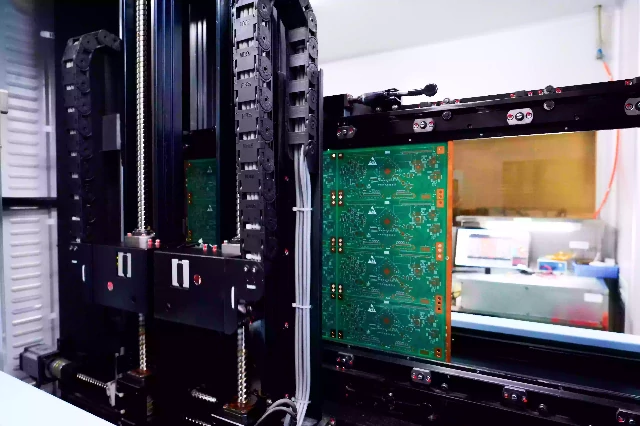
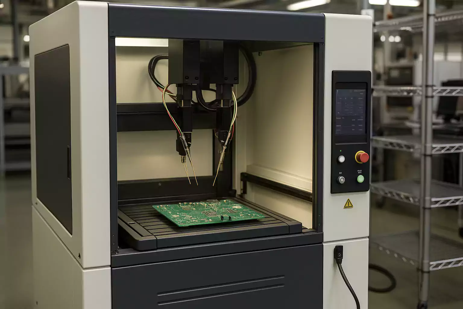
How Does Flying Probe Testing Work?
Flying probe systems typically consist of:
- Multiple robotic probes (usually 2–8) mounted on high-precision arms
- X-Y-Z gantry system to move the probes across the board surface
- Automated test software that reads CAD/Gerber/netlist files and generates the test plan
- Optional camera systems for component recognition and alignment
- Integrated measurement instruments for checking voltage, current, resistance, and continuity
The test begins by importing the PCB's design files into the system. The software automatically identifies all available test points and determines the optimal probe path. The probes then move rapidly across the surface of the board, making sequential electrical contacts at designated locations.
Types of Boards Tested with FPT
Flying Probe Testing can be applied to:
- Bare boards (bare PCB testing): For checking open/short circuits, net continuity, and trace integrity before assembly.
- Assembled boards (PCBA): To verify component presence, polarity, orientation, and basic electrical values after SMT or through-hole assembly.
This versatility allows manufacturers to use the same test platform across different stages of production without needing to invest in additional hardware.
Key Characteristics of a Flying Probe System
| Feature | Description |
|---|---|
| Fixtureless | No need for custom test fixtures, reducing cost and setup time |
| CAD-driven | Uses design files to auto-generate test programs |
| High precision | Suitable for fine-pitch, high-density boards |
| Configurable probes | Can test top, bottom, or both sides of the PCB |
| Ideal for low volumes | Cost-effective for small batches and prototypes |
Key Advantages of Flying Probe Testing
Flying Probe Testing has become a go-to solution for electronics manufacturers dealing with prototype validation, low-volume production, and frequent design revisions. Its unique capabilities offer a level of flexibility and cost-efficiency that traditional fixture-based test methods simply cannot match.
Here are the core advantages that make flying probe testing a smart choice for modern PCB testing workflows:
1. No Fixture Required – Save Time and Cost
Traditional In-Circuit Testing (ICT) systems require expensive, custom-built fixtures that can take days or weeks to fabricate. Flying probe testers eliminate this entirely. With no need for mechanical test fixtures, you can:
- Begin testing within hours of receiving the board design
- Avoid the upfront fixture cost (which can exceed $5,000 per design)
- Easily handle frequent design changes without retooling
This makes flying probe testing ideal for rapid prototyping and NPI (New Product Introduction).
2. Extremely Fast Turnaround for New Designs
Flying probe systems use software to generate probe paths directly from your CAD or Gerber files. This enables test programs to be created in a matter of hours, drastically reducing time-to-test. For projects with tight development cycles, this speed is invaluable.
3. Highly Flexible and Adaptable
Because the probes are controlled via motors, flying probe testers can adapt to different board layouts, component densities, and even unconventional geometries. This makes them especially useful for:
- Small batches of different board types
- High-mix, low-volume (HMLV) production environments
- Testing boards with limited or irregular test point access
4. Safe, Non-Destructive Testing
Flying probe testing is a non-invasive, non-destructive method that applies minimal mechanical stress to the PCB. This is crucial when working with:
- Fragile components
- Flexible PCBs (FPCs)
- Boards with sensitive or high-value circuitry
5. Double-Sided and High-Density Board Support
Modern flying probe systems are capable of accessing both the top and bottom layers of a PCB without flipping the board or using complex fixtures. This allows for full test coverage of:
- HDI (High-Density Interconnect) boards
- BGA, QFN, and other fine-pitch components
- Vias, microvias, and through-hole pins
6. Comprehensive Test Coverage
Flying probe testers can perform a wide range of electrical tests, including:
- Open/short detection
- Resistance and continuity checks
- Capacitance measurements
- Diode polarity and LED functionality
- Power rail verification
With high pin accuracy and configurable probe force, the system ensures precise contact with even the smallest pads.
7. Built-in Diagnostics and Reporting
Most flying probe testers come equipped with powerful software tools that automatically generate:
- Detailed fault reports
- Net-level diagnostics
- Visual mapping of test results
- Statistical process control (SPC) data
This makes debugging and process validation faster and more accurate—greatly improving design and manufacturing feedback loops.
8. Ideal for Design Iteration and R&D
When you're rapidly evolving a design, test adaptability becomes essential. Flying probe testing allows you to:
- Reuse existing test programs with minimal changes
- Modify test conditions on the fly
- Reduce time lost in test setup and fixture modifications
This leads to faster iterations and higher-quality prototypes.
Limitations and Challenges of Flying Probe Testing
While Flying Probe Testing (FPT) offers unmatched flexibility and convenience for low-volume PCB testing, it’s not without its trade-offs. Understanding the limitations and operational challenges of flying probe systems is critical for choosing the right test strategy, optimizing board design, and setting realistic expectations for performance and throughput.
1. Slower Test Speeds for High-Volume Production
Flying probe testers rely on mechanical movement to access test points one (or a few) at a time. Unlike In-Circuit Testing (ICT) systems that can evaluate hundreds of nets simultaneously, flying probes test each net sequentially. This means that as board complexity or quantity increases, total test time can rise significantly. For high-volume production environments, this can become a bottleneck in the manufacturing line.
2. Limited Access to Certain Components and Nets
Flying probes require physical access to test points or component leads. If a net is hidden under a component (e.g., under a BGA) or lacks a dedicated test pad, it may be impossible to probe without special accommodations. Boards with dense layouts, buried vias, or poor testability can suffer from limited test coverage.
3. Mechanical Wear and Probe Contact Reliability
Probes are delicate mechanical components that repeatedly contact small pads, often only a few millimeters wide. Over time, probe tips can wear down, bend, or become contaminated, which affects contact reliability and can lead to false failures (false negatives) or missed defects (false positives).
4. Not Suitable for Functional Testing Out-of-the-Box
Standard flying probe systems primarily conduct electrical continuity and isolation tests. While some advanced models support optional functional testing (FCT) modules, these are often limited and may require additional setup or instrumentation. For products that require power-on testing, simulations, or performance validation, flying probe alone is usually insufficient.
5. Challenging for Ultra-Small Pads or Tight Spaces
As PCB designs trend toward smaller geometries and tighter component spacing, probe access becomes more difficult. Probing extremely small test pads (<0.4 mm diameter) or navigating between closely packed components without damaging surrounding areas can be challenging even for high-precision probe systems.
6. Requires Expert Setup for Accurate Results
While flying probe testing is known for being fast to set up compared to fixture-based methods, achieving optimal fault coverage and reliable performance still requires skilled engineers. The quality of CAD data, netlists, and test strategy definition has a significant impact on test effectiveness.
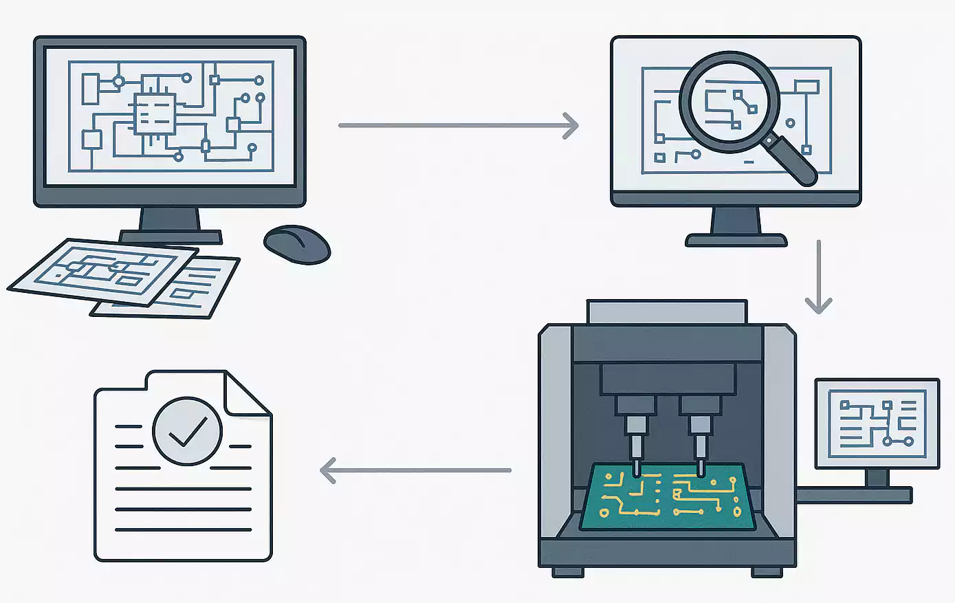
Flying Probe Testing Workflow Explained
Understanding the flying probe testing workflow is essential for engineers and manufacturers looking to optimize their production process and ensure high board quality—especially during prototype and low-volume PCB runs. While flying probe systems eliminate the need for fixtures, they still follow a structured, data-driven testing process that ensures accuracy, repeatability, and reliability.
Here’s a step-by-step breakdown of how flying probe testing works from start to finish:
Step 1: Data Preparation
Before testing begins, the manufacturer must provide a complete set of design files, which typically includes:
- CAD data (ODB++, IPC-2581, or ASCII format)
- Gerber files
- Bill of Materials (BOM)
- Netlist or test-point list
These files are used to map all testable nodes on the PCB and define where probes need to land. The better the data quality, the more accurate and efficient the testing process will be.
Step 2: Test Program Generation
Using the provided files, the flying probe system software automatically generates a test program. This includes:
- Probe movement paths (optimized to minimize travel time)
- Electrical test sequences (continuity, isolation, resistance, etc.)
- Component-level checks if testing an assembled board (PCBA)
Many modern systems allow for simulation and dry runs before actual testing, helping identify unreachable nets or missing data before wasting time on physical boards.
Step 3: Board Setup and Alignment
The PCB is loaded onto the machine—manually or via automated loader depending on system capability. High-precision cameras or fiducial marks are used to align the board accurately to the probe coordinates.
Double-sided testing systems may require flipping or dual probe heads, allowing for seamless access to both top and bottom layers.
Step 4: Probing and Electrical Testing
The testing process begins as multiple flying probes move across the board in a precise, coordinated manner. The system performs a range of tests, such as:
- Open/short detection
- Continuity verification
- Passive component measurement (R, C, L)
- Polarity checks for diodes
- Insulation resistance
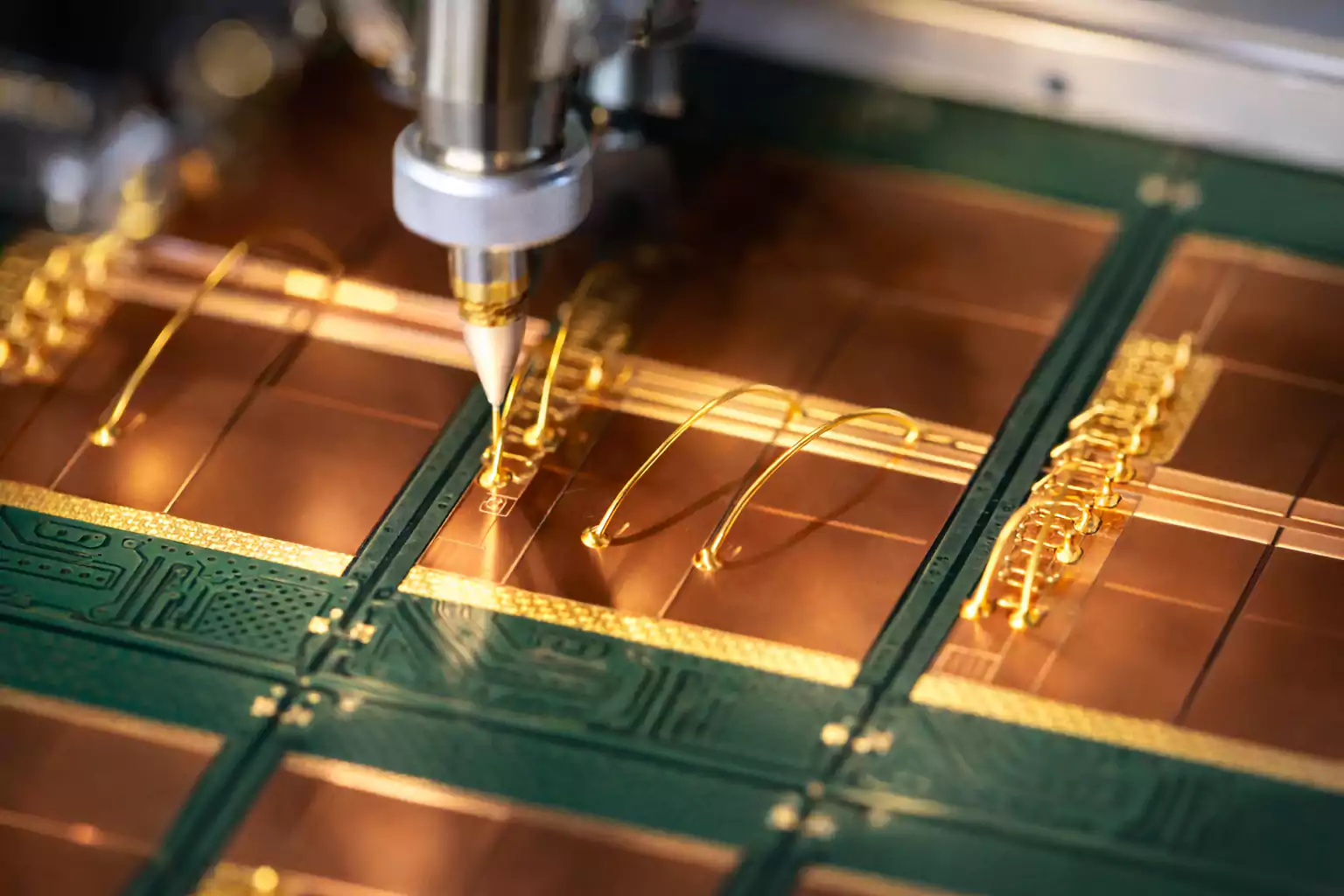
Probes typically make contact with test pads, vias, or exposed traces. Contact pressure, probe angle, and dwell time are automatically controlled to ensure reliable results without damaging the board.
Step 5: Fault Detection and Reporting
Once testing is complete, the system automatically generates a detailed report outlining:
- Pass/fail status
- Pin or net-level failure details
- Measurement values
- Test coverage metrics
This report can be exported in various formats (PDF, CSV, XML) and integrated into manufacturing execution systems (MES) for traceability.
Step 6: Debugging and Feedback Loop
In case of test failures, the report helps engineers quickly locate the faulty net or component. This enables immediate corrective action—be it design modification, manual inspection, or rework.
Flying probe testing supports an iterative design process by feeding valuable electrical performance data back to the development team, helping improve yield and accelerate time-to-market.
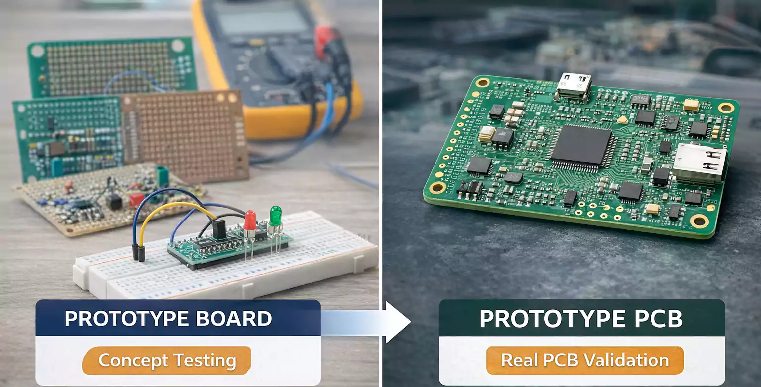
How to Prepare Your PCB Design for Flying Probe Testing (Design for Testability)
To fully benefit from Flying Probe Testing (FPT), it’s essential to design your PCB with testability in mind. While FPT doesn’t require a custom fixture, it still relies on the availability and accessibility of electrical nodes on the board. Poor test point design, limited probe access, or unclear layout documentation can significantly compromise test coverage and accuracy.
This section focuses on practical design guidelines to ensure your PCB is optimized for flying probe testing, helping reduce false failures, improve yield, and minimize debugging time.
1. Prioritize Accessible Test Points
Flying probe systems work best when clear, unobstructed access to electrical nodes is provided. Consider the following:
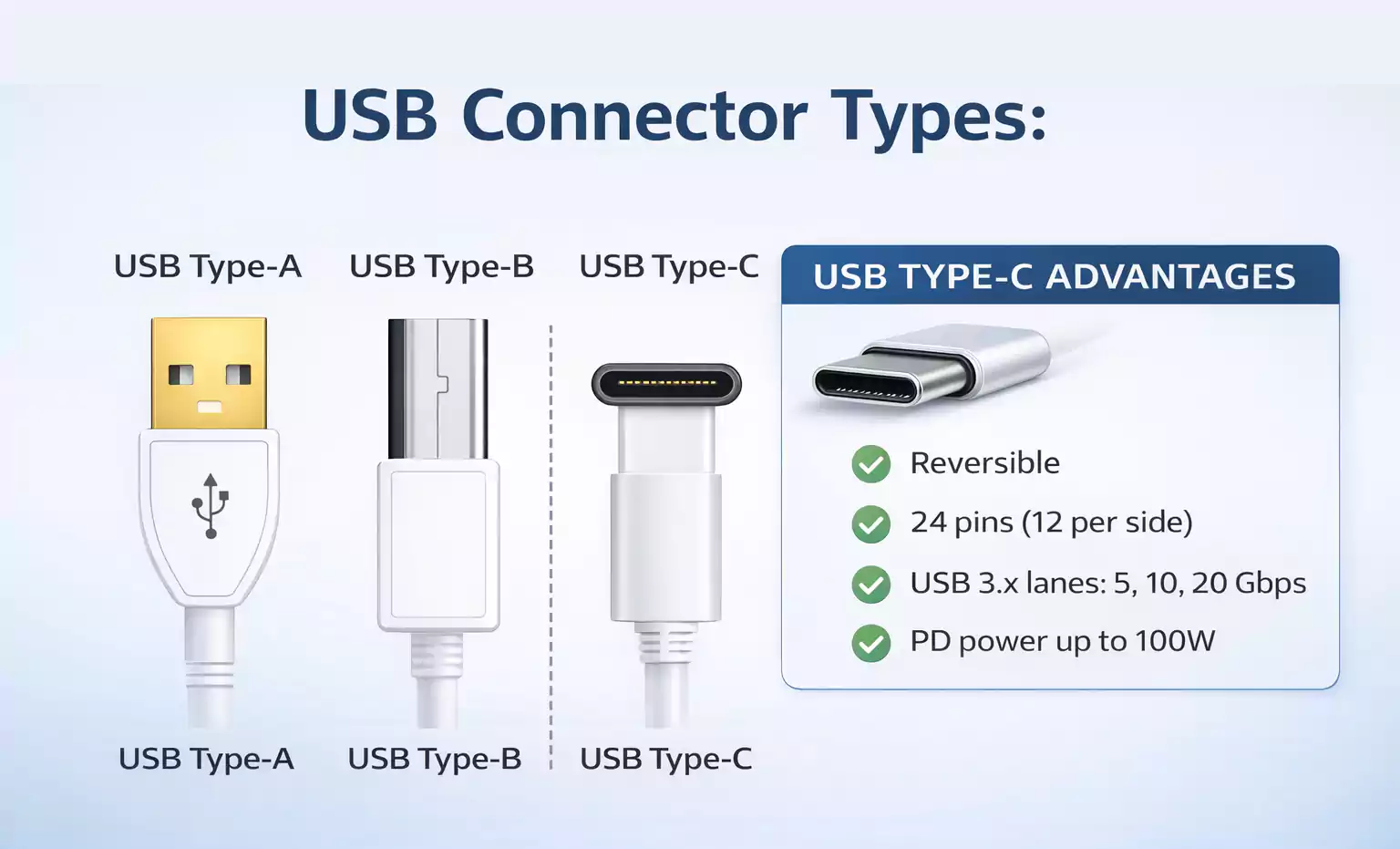
- Pad size: Ensure test pads are at least 0.5 mm in diameter for reliable probe contact.
- Pad spacing: Maintain a minimum of 1 mm between test points to avoid probe interference.
- Avoid solder mask over pads: Use mask openings to expose test pads for contact.
For double-sided boards, make sure critical nets have accessible pads on either side. This increases the flexibility of probe path generation.
2. Label Critical Nets and Component Polarities
FPT software often uses net names and design labels for automated test generation. Ensure the following are clearly defined in your design files:
- Net names for power, ground, and signal lines
- Diode and LED polarities
- Orientation for polarized capacitors and ICs
- Reference designators aligned to actual component locations
Well-documented design data not only improves test coverage but also reduces manual setup and debugging time.
3. Minimize Probe Shadowing and Physical Obstructions
Components like large connectors, heatsinks, or tall components can block probe access to nearby test pads.
Best practices include:
- Avoid placing tall components near small test pads
- Maintain clearance zones around critical test areas
- Consider placing test points on inner zones for complex components (if outer pins are unreachable)
If you’re using BGAs or dense ICs, provide breakout vias or pads to allow at least minimal probing of those nets.
4. Supply Complete, Clean Design Data
To allow the test house or in-house team to generate flying probe programs accurately, always provide:
- Gerber files (layers + solder mask)
- Complete BOM with component values and tolerances
- Netlist or IPC-D-356 format (to validate connectivity)
- Assembly drawings with component placement info
- Any known design limitations or areas not to be probed
Clean, well-structured design data significantly reduces back-and-forth communication and leads to faster test setup.
5. Plan for Testability Early in the Design Cycle
Design for Testability (DFT) is most effective when considered from the beginning—not after layout completion. Early-stage planning can ensure:
- Adequate spacing for probe contact
- Strategic placement of test pads for critical nets
- Inclusion of optional test pads for future revisions
- Alignment with your chosen test method (FPT in this case)
By making testability a priority during schematic and layout phases, you’ll avoid costly redesigns and increase first-pass yield during validation.
Cost and Turnaround Time Evaluation: Is Flying Probe Testing Worth It?
One of the most attractive features of Flying Probe Testing (FPT) is its low upfront cost and fast setup time, especially compared to fixture-based testing methods like In-Circuit Testing (ICT). But how does it truly stack up in real-world cost and scheduling scenarios?
Let’s break down what you need to consider.
1. Cost Structure of Flying Probe Testing
Unlike ICT or functional test setups that require custom-built fixtures—often costing hundreds or even thousands of dollars—flying probe testers use software-defined probe paths, eliminating tooling expenses entirely.
Typical cost components include:
- Programming/Setup Fee: Usually a flat fee per job, often ranging from $50–$200 depending on complexity.
- Per-Unit Testing Fee: Generally ranges from $1–$5 per board, based on board size, density, and test point access.
- Optional Add-Ons: Some providers charge extra for additional test coverage (e.g., component value checks, BGA access analysis, high-voltage testing).
2. Turnaround Time Advantages
Because FPT doesn't require hardware setup or fixture manufacturing, lead times are dramatically reduced. This is especially useful during the prototyping phase or when rapid design iterations are necessary.
| Test Method | Setup Time | Testing Speed | Total Turnaround (typical) |
|---|---|---|---|
| Flying Probe | < 1 day | Moderate (per board) | 1–3 days |
| ICT | 5–10 days (fixture build) | Fast (parallel pins) | 6–12 days |
| AOI | 1–2 days | Fast | 2–4 days |
3. When FPT Is Most Cost-Effective
Flying Probe Testing delivers the best ROI in the following scenarios:
- Prototype validation: Minimal cost to get testing started within a day
- Low-volume production (10–500 units): Lower total test cost compared to fixture-based alternatives
- Frequent design revisions: Avoids the sunk cost of discarded or modified test fixtures
- High-mix production: Short setup time allows fast switching between board variants
4. Scaling Cost: A Realistic Example
Here’s a simplified cost comparison to illustrate how FPT scales across different volumes:
| Volume | FPT Setup ($) | FPT Per Unit ($) | Total FPT Cost | ICT Fixture ($) | ICT Per Unit ($) | Total ICT Cost |
|---|---|---|---|---|---|---|
| 10 pcs | 100 | 2.00 | $120 | 1000 | 0.50 | $1005 |
| 100 pcs | 100 | 2.00 | $300 | 1000 | 0.50 | $1050 |
| 1000 pcs | 100 | 2.00 | $2100 | 1000 | 0.50 | $1500 |
5. Hidden Costs to Watch For
While FPT minimizes many traditional expenses, some hidden costs may still apply:
- Design revisions during testing: Changes after program generation may require reprogramming fees
- Test access limitations: Poorly accessible test points could increase manual rework time
- Extra time for high-density PCBs: Boards with more test nodes take longer per unit, increasing per-board cost
Use Cases and Real-World Applications of Flying Probe Testing
Flying Probe Testing (FPT) is not just a theoretical solution—it’s widely used across industries where speed, flexibility, and precision are critical during the early stages of electronics development. Because it eliminates the need for custom fixtures and adapts quickly to design changes, flying probe testing is ideal for various real-world manufacturing scenarios.
1.Prototype Validation in R&D and NPI
One of the most common applications for flying probe testing is prototype validation during new product introduction (NPI). Engineering teams often need to test multiple board iterations in a short timeframe, and fixture-based testing simply isn’t practical due to its setup cost and lead time.
Use case example:
A medical device manufacturer developing a wearable ECG unit used flying probe testing to validate four board revisions over six weeks. The FPT system allowed them to catch short circuits and missing components without delaying their clinical trial schedule.
2.Low-Volume Production Testing
When producing PCBs in small batches—such as for pilot runs, regional product variants, or customized industrial controls—flying probe testing offers a cost-efficient way to maintain quality. The per-board test time is acceptable when volume is under 200–300 units, and the lack of fixture investment keeps total cost low.
Use case example:
An automotive startup launched a low-volume run of smart battery management PCBs. They used flying probe testing to ensure 100% functional verification without incurring the $10,000+ fixture cost typical of in-circuit testing (ICT).
3.High-Mix, Low-Volume (HMLV) Environments
Contract manufacturers (CMs) who serve multiple customers often operate in high-mix, low-volume production environments. Flying probe testers are highly versatile and can test many different board designs with minimal switchover time.
Use case example:
An EMS provider working with aerospace and defense contractors uses a single flying probe line to test over 50 different board SKUs per month, avoiding the complexity of managing dozens of ICT fixtures.
4.Failure Analysis and Engineering Debug
FPT is often used in failure analysis labs and engineering departments to diagnose issues on failed boards returned from the field. Since the test system can be programmed from the board data alone, it's a powerful tool for non-destructive troubleshooting without relying on existing fixtures.
Use case example:
A network hardware company used flying probe testing to isolate cold solder joints in boards returned from customer installations. The probe's high-precision movement and force control helped them find intermittent faults that weren’t visible under AOI or X-ray inspection.
Conclusion: Elevate Your PCB Prototyping with Flying Probe Testing
Flying Probe Testing (FPT) offers a highly flexible and fixture-free solution for testing prototypes and low-volume PCBs. With minimal setup time and strong test coverage, it's ideal for fast-moving projects and frequent design changes.
By integrating flying probe testing early in the development process, engineers can catch electrical issues before they escalate—saving time, reducing costs, and improving product reliability.
To get the most out of FPT:
- Apply Design for Test (DFT) principles during layout
- Share complete design data with your test provider
- Use FPT as part of a broader test strategy when needed
As PCB designs grow more complex, adopting flying probe testing is no longer optional—it’s a smart investment for speed, precision, and quality.