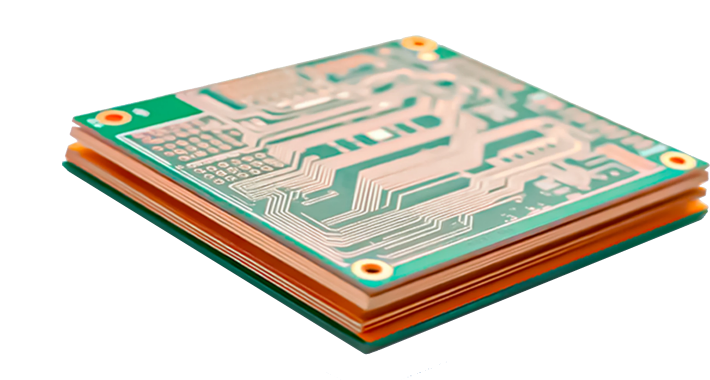
مصنع نماذج أولية للوحات الدوائر المطبوعة
خدمات تصنيع النماذج الأولية السريعة والكميات الكبيرة من لوحات الدوائر المطبوعة المرنة
بصفتنا موردًا رائدًا للوحات الدوائر المطبوعة المرنة في الصين، فإننا متخصصون في تصنيع الدوائر المرنة عالية الجودة، بدءًا من النماذج الأولية السريعة وصولاً إلى الإنتاج الكامل للوحات الدوائر المطبوعة المرنة. حمّل ملفات Gerber الخاصة بك الآن للحصول على عرض سعر سريع وموثوق.


ما هو تصميم النماذج الأولية للوحات الدوائر المطبوعة؟
تتضمن عملية تصميم النماذج الأولية للوحات الدوائر المطبوعة إنتاج دفعة صغيرة من اللوحات بسرعة من ملفات التصميم قبل الإنتاج الضخم، وذلك للتحقق من صحة الوظائف واختبار الأداء وتقييم العملية. تُمكّن هذه النماذج الأولية المهندسين من اكتشاف عيوب التصميم بسرعة وتحسين التخطيطات، مما يضمن تصنيعًا واسع النطاق خاليًا من العيوب.
لماذا تختار خدمة تصنيع نماذج لوحات الدوائر المطبوعة لدينا؟
Standard lead time of 5–7 business days; 3‑day expedited delivery for urgent R&D needs.
Minimum line width/spacing of 4 mil; hole sizes down to 0.2 mm; supports multilayer, flex, and HDI boards.
IPC-610 compliant with AOI, ICT, and X-ray inspections—100% coverage to eliminate manufacturing defects.
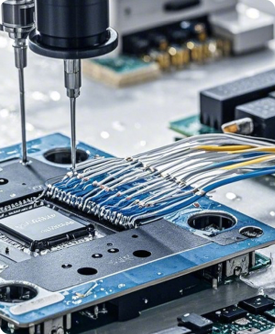
From prototyping and SMT assembly to stencil fabrication and DFM checks, streamlining communication and shortening project cycles.
العملية وسير العمل
الخطوة 1
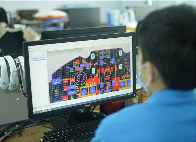
تقديم التصميم
- تحميل ملفات Gerber/CAD
- يدعم تنسيقات Gerber 274X و ODB++ و IPC-2581.
- يتم أرشفة الملفات تلقائيًا باستخدام معرف مشروع فريد.
الخطوة الثانية
المراجعة الفنية
- التقييم اليدوي خلال ساعتين.
- الفحوصات الرئيسية: الحد الأدنى لعرض/تباعد الخطوط، قطر الثقوب، فتحات قناع اللحام، والمسافة الفاصلة لقناع اللحام.
- تم إصدار اقتراحات التحسين وتأكيدها عبر البريد الإلكتروني أو الهاتف.
الخطوة 3
النماذج الأولية والتصنيع
- إعداد خط الإنتاج: عمليات حفر باستخدام آلات التحكم الرقمي الحاسوبي المؤتمتة بالكامل وتصفيح نحاسي عالي الدقة.
- دعم عمليات التصنيع: لوحات أحادية/مزدوجة الجوانب، متعددة الطبقات، مرنة، ولوحات عالية الكثافة (HDI).
- رقابة بيئية صارمة: يمنع تنظيم درجة الحرارة والتنظيف الشامل التلوث ويضمن الحصول على أسطح مستوية ومتجانسة.
الخطوة الرابعة
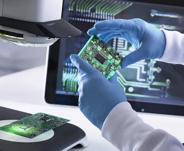
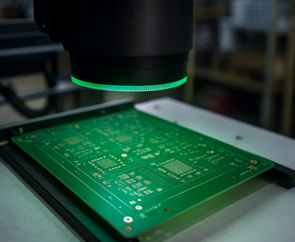
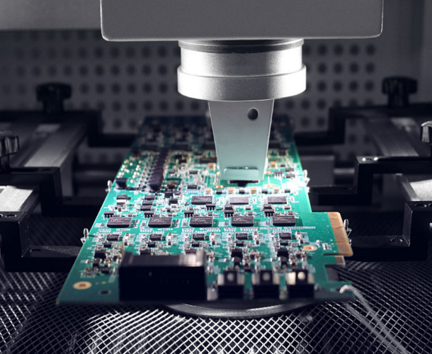
فحص الجودة
- نظام فحص بصري آلي بنسبة 100%: يكتشف فورًا الدوائر المفتوحة والدوائر القصيرة والوصلات المفقودة.
- اختبار الدوائر المتكاملة (ICT): يشمل نقاط الاختبار الشبكية لضمان سلامة الإشارة بشكل كامل.
- فحص الطبقات بالأشعة السينية: يتحقق من سلامة الثقوب المخفية/المدفونة وجودة عملية الترقق.
الخطوة 5
الشحن والدعم
- تغليف مفرغ من الهواء مضاد للكهرباء الساكنة مع مادة مجففة.
- شركات شحن متعددة: EMS، DHL، UPS، جميعها توفر خدمة تتبع كاملة للشحنات.
- يتم إرسال رقم التتبع خلال 24 ساعة من الشحن، ويتوفر دعم فني عبر الإنترنت على مدار 12 ساعة يوميًا، سبعة أيام في الأسبوع.

القدرات
| القدرة | المعايير | التفاصيل |
|---|---|---|
| الطبقات | ما يصل إلى 50 طبقة | نماذج أولية عالية الكثافة متعددة الطبقات (حتى 50 طبقة)، مثالية لتطبيقات الاتصالات والفضاء والدفاع. |
| الحد الأقصى للحجم | 600 × 500 مم | أقصى حجم للوحة: 600 × 500 مم، يدعم تطبيقات التحكم الصناعي واسعة النطاق، وشاشات LED، والإلكترونيات الخاصة بالسيارات. |
| السماكة | 0.2 - 7.0 ملم | سماكة اللوحة: 0.2 ملم - 7.0 ملم، من الألواح المرنة فائقة الرقة (للتطبيقات القابلة للارتداء) إلى ركائز الألومنيوم الصلبة (عالية الصلابة). |
| سمك النحاس | 0.33 - 12 أونصة | وزن النحاس: 0.33 - 12 أونصة، من لوحات الدوائر الكهربائية القياسية إلى لوحات الطاقة عالية التيار مع تحسين تبديد الحرارة. |
| الحد الأدنى لعرض الخط / المسافة بين الخطوط | 2.5 مل / 2.5 مل | الحد الأدنى لعرض الخط / المسافة بين الخطوط 2.5 مل، يدعم مسافات بين الرقائق والحزم تصل إلى 0.5 مم أو أقل لتقنية التجميع السطحي عالي الكثافة |
| أصغر قطر لثقب الحفر | 6 مل | أصغر قطر للحفر 6 مل، يتيح إنشاء ثقوب توصيل دقيقة مخفية/مدفونة لدوائر التوصيل عالية الدقة للترددات الراديوية والموجات الدقيقة. |
| خلوص الفتحة إلى المسار | ٥ مل | الحد الأدنى للحلقة الحلقية ٥ مل، مطابق لمعايير IPC-2221 لتقليل التداخل بين المسار والفتحة |
| تحمل المعاوقة | ±10% أو ±5% | معاوقة محكومة بدقة ±5% (±10% اختياري)، مناسبة لإشارات عالية السرعة (USB3.0، PCIe، RF) والدوائر الرقمية القياسية |
| تفاوت الأبعاد | ±0.1 مم | يضمن تفاوت الأبعاد الخارجية البالغ ±0.1 مم دقة ميكانيكية عالية للتجميعات الصناعية والاستهلاكية التي تتطلب ملاءمة محكمة. |
| المواد | Shengyi S1000 2، S1141، ITEQ IT180A، مواد أساسها الألومنيوم والنحاس، سلسلة Rogers RF (4350B، 4003C، 3003)، سلسلة RT/VT، DuPont PI، سلسلة ISOLA FR، Megtron 4/6 | خيارات المواد: FR-4، الألومنيوم، النحاس، مواد عالية التردد (Rogers، Megtron)، ومواد مرنة من نوع PI |
| حجم فتحة الغطاء الواقي | ≥ 0.6 مم × 0.6 مم | نافذة الغطاء الواقي المرن بحد أدنى 0.6 × 0.6 مم، تضمن قوة التصاق ومتانة عالية للطبقات في الأجهزة القابلة للارتداء وأجهزة الاستشعار الطبية التي تتعرض للانحناء المتكرر. |
| معالجة السطح | ENIG، ENEPIG، I Ag، OSP، HAL (خالي من الرصاص)، طلاء ذهب رقيق، طلاء ذهب صلب |
حالات الاستخدام في الصناعة

لوحات النماذج الأولية للفضاء والدفاع
- التطبيقات: موثوقية عالية المستوى في قطاعي الطيران والدفاع، وتصميمات متعددة الطبقات عالية الكثافة، والتحكم الدقيق في المعاوقة.
- الميزات: متوافقة مع معيار IPC-6012 الفئة 3، تحمل مقاومة بنسبة ±5%، تشطيب ENIG.

نماذج أولية للأجهزة الطبية
- التطبيقات: دوائر مصغرة عالية الكثافة للأجهزة الطبية التي تتطلب مواد متوافقة حيوياً ولوحات دوائر رقيقة للغاية.
- الميزات: عرض خط أدنى يبلغ 2.5 مل، ركيزة مرنة من مادة البولي إيميد، فحص آلي بصري وفحص الدوائر المتكاملة بنسبة 100%.

نماذج أولية للإلكترونيات في مجال السيارات
- التطبيقات: دوائر مصغرة عالية الكثافة للأجهزة الطبية التي تتطلب مواد متوافقة حيوياً ولوحات دوائر رقيقة للغاية.
- الميزات: عرض خط أدنى يبلغ 2.5 مل، ركيزة مرنة من مادة البولي إيميد، فحص آلي بصري وفحص الدوائر المتكاملة بنسبة 100%.

إنترنت الأشياء والإلكترونيات الاستهلاكية
- التطبيقات: التطوير السريع لأنظمة المنزل الذكي والأجهزة القابلة للارتداء والإلكترونيات الاستهلاكية.
- الميزات: يدعم لوحات الدوائر المطبوعة فائقة النحافة بسمك 0.2 مم، والتكامل المرن والصلب، وتقديم خدمات متعددة العمليات من خلال جهة واحدة.

التعليمات
The manufacturing time of PCB prototypes varies due to various factors, including the complexity of the circuit board, the manufacturing plant’s production capacity, and order volume.
Generally speaking, simple single or double-sided board prototypes can be manufactured in a few days, while complex multi-layer boards or circuit boards containing special processes such as blind holes and buried holes may require longer time.
To shorten the manufacturing cycle, it is recommended to choose PCB manufacturers with advanced manufacturing equipment and efficient production processes.
Poor circuit: such as open circuit, short circuit, circuit width or spacing not meeting design requirements, etc.
Pad issues: Pad detachment, incorrect pad size, mismatch between pad and component pins, etc.
Drilling problems: aperture deviation, incorrect hole position, poor hole wall quality, etc.
Surface treatment defects: such as uneven coating of solder mask, blurry character printing, insufficient coating thickness, etc.
These issues may be caused by design errors, improper process control during manufacturing, or material quality problems.
Therefore, a detailed design review should be conducted before manufacturing, reliable manufacturers should be selected, and strict quality control should be implemented during the manufacturing process.
Manufacturing capability: Does the manufacturer have advanced manufacturing equipment and processes to meet your design requirements and production capacity needs.
Quality control: Whether the manufacturer has established a sound quality management system and can provide reliable quality assurance and after-sales service.
Price and delivery time: Compare the prices and delivery times of different manufacturers and choose the manufacturer with high cost-effectiveness.
Technical support: Does the manufacturer provide technical support and solutions, and can they assist in solving problems during the design or manufacturing process.
Electrical performance: The dielectric constant, dielectric loss, resistivity, and other electrical properties of the material should meet the design requirements.
Mechanical strength: The mechanical properties such as bending strength and impact strength of the material should be sufficient to ensure the reliability and durability of the circuit board.
Thermal stability: The material should have good thermal stability and be able to withstand certain temperature changes without deformation or cracking.
Processing performance: The material should be easy to process, such as drilling, etching, electroplating, and other processes should be able to proceed smoothly.
Cost: While ensuring performance, the cost of materials should be considered and materials with high cost-effectiveness should be selected.
Electrical testing: Check the conductivity, insulation resistance, withstand voltage and other electrical performance of the circuit.
Functional testing: Verify whether the circuit board works according to design requirements, including signal transmission, power distribution, and other functions.
Reliability testing: such as thermal cycling testing, wet heat testing, vibration testing, etc., to evaluate the reliability of circuit boards during long-term use.
Appearance inspection: Check the appearance quality of the circuit board, such as solder joint quality, solder mask coating, character printing clarity, etc