Leitfaden „PCB Fabrication Low Cost“ 2026: Sparen, ohne Qualität zu opfern
Leitfaden für kostengünstige Leiterplattenfertigung: Kluge Entscheidungen bei Materialien, Dicke, Oberflächenveredelung, Tests und Lieferzeiten, plus Lieferantenrankings für 2026 – erschwingliche Leiterplatten ohne Risiko.
Quick Turn PCB & Assembly in the USA – 24–72 Hour Prototypes Done Right (DE-Übersetzung)
Erfahren Sie, wie Sie in den USA zuverlässige Leiterplatten und Leiterplattenbestückungen mit kurzer Lieferzeit erhalten – Prototypen in 24–72 Stunden, schlüsselfertige Lösungen, praktische DFM-Tipps und wie Sie die Lieferzeit verkürzen können, ohne die Qualität zu beeinträchtigen.
Leiterplatten Oberflächenfinish: ENIG vs. HASL vs. OSP & mehr – Welche ist die beste für Ihre Platine?
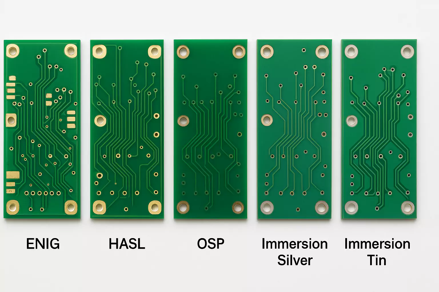
Vergleichen Sie die gängigsten Leiterplatten Oberflächenfinish – ENIG, HASL, OSP, Immersion Silver und Immersion Tin. Erfahren Sie, wie sich jede davon auf Lötbarkeit, Kosten, Zuverlässigkeit und RoHS-Konformität auswirkt, um das optimale Finish für Ihr Leiterplattendesign auszuwählen
Lötmasken- und Siebdruckverfahren
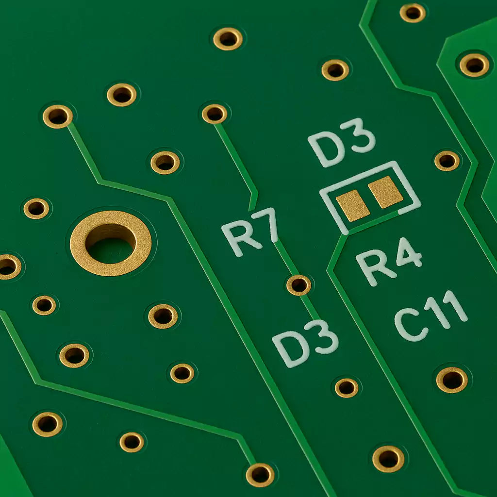
Entdecken Sie, wie sich Lötstoppmasken und Siebdruckschichten auf die Zuverlässigkeit von Leiterplatten auswirken. Dieser Leitfaden behandelt wichtige Prozessschritte, bewährte Designmethoden und zeigt, wie Sie häufige Probleme wie Pad-Fehlausrichtung und Siebdrucküberlappung vermeiden.
PCB Drilling and Plated Through Holes
Learn everything about PCB drilling and plated-through holes—including drilling methods, plating processes, quality factors, common defects, and DFM guidelines to avoid manufacturing issues.
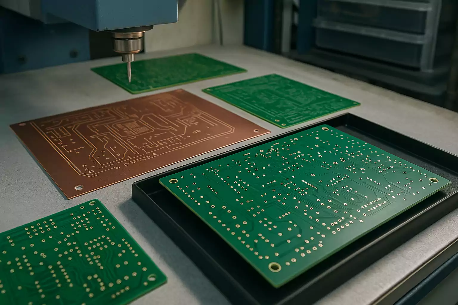
Inner Layer Imaging and Lamination
Learn how inner layer imaging and lamination shape the quality and reliability of multilayer PCBs. This expert guide covers photoresist patterning, etching, material shrinkage, stack-up design, and process control—essential for engineers optimizing multilayer board performance.
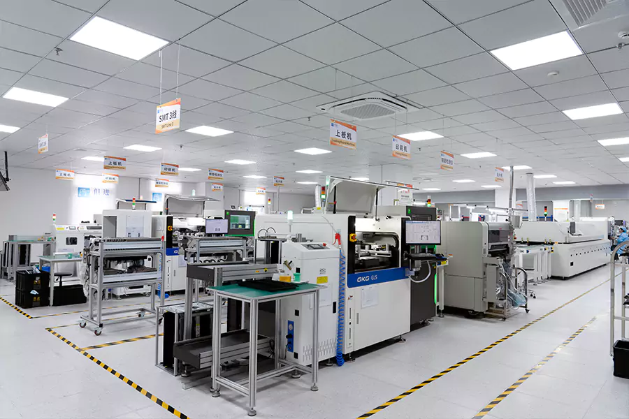
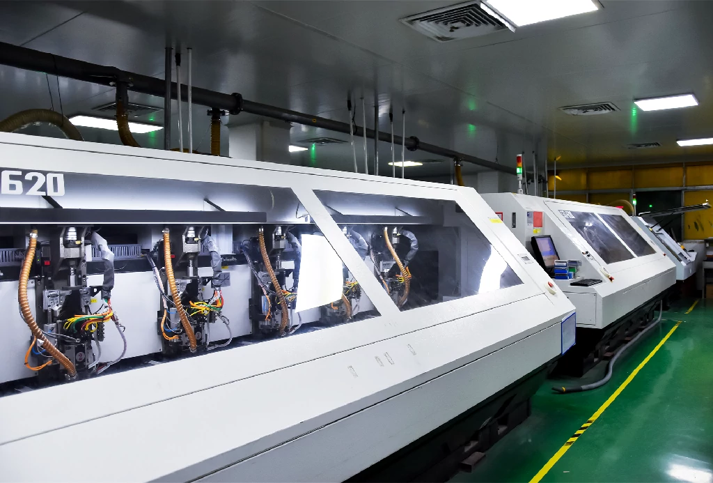
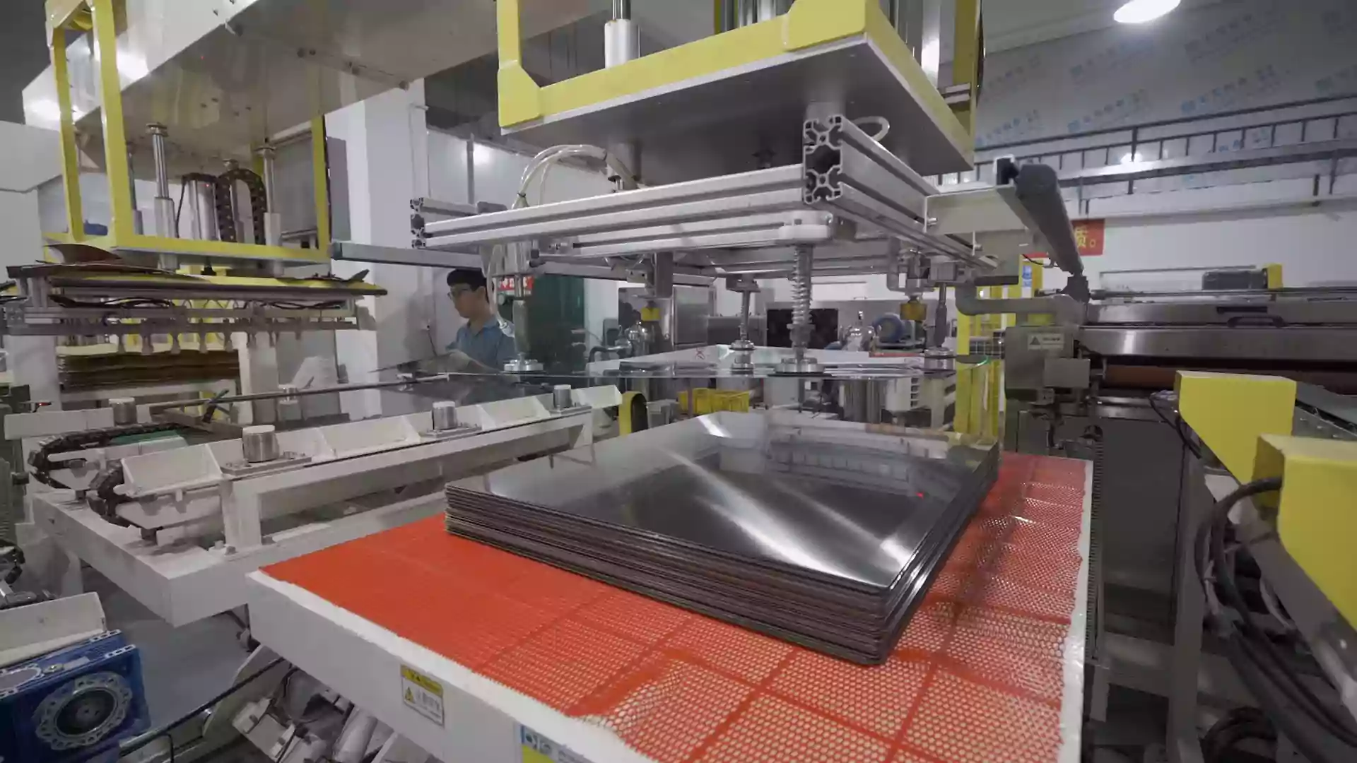
Full Overview of PCB Manufacturing Process
Explore the complete PCB manufacturing process—from design files to finished boards. Learn every key step including imaging, drilling, plating, solder mask, and testing. Ideal for engineers and teams seeking reliable, high-quality PCB production.